Chapter 11 — Band structures
Once you have solved the Kohn–Sham equations for a periodic solid, you are left with a list of energies that depend on a continuous variable k in the Brillouin zone. This chapter is about what to do with that list.
By the end of chapter 07 we had a Kohn–Sham Hamiltonian at every crystal momentum k in the first Brillouin zone, and we could solve the eigenproblem $H(\mathbf k) \psi_{n\mathbf k} = \varepsilon_{n\mathbf k} \psi_{n\mathbf k}$ to obtain a discrete set of eigenvalues at each k. The result is a set of continuous functions $\varepsilon_n(\mathbf k)$ — the band structure of the solid — and a discrete Fermi energy $\varepsilon_F$ chosen so that exactly $N_e$ states are filled. Everything else in this chapter is a way of compressing the band structure into a finite number of useful quantities: a band-structure plot along a 1-D k-path, a density of states (DOS) as a function of energy, a projected DOS onto atomic orbitals, a 2-D or 3-D Fermi surface, an effective mass tensor, an orbital character, a spin–orbit splitting. Each of these compressions is a small loss of information but a large gain in interpretability: the band-structure plot is the universal fingerprint of a solid, and reading it correctly is the single most useful skill in solid-state DFT.
Reading note. This chapter assumes you have read chapters 01–07. It uses the plane-wave machinery of chapter 06 and the Bloch / Brillouin-zone / k-point sampling machinery of chapter 07 without re-deriving them. Forward cross-references: the projected DOS is the basis of the projected-crystal-field analysis in the transition-metal chapters that follow, and the Fermi-surface language is reused in the transport discussion.
11.1 The claim
The Kohn–Sham band structure. Let $V_\text{eff}\rho$ be the self-consistent Kohn–Sham effective potential of chapter 04, evaluated at the ground-state density of a crystal. Let $\mathbf k$ be a point in the first Brillouin zone. The Kohn–Sham eigenproblem on the plane-wave basis of chapter 07 is \(\begin{equation} \label{eq:ch-11-ks-eig} H(\mathbf k) \, \mathbf c_{n\mathbf k} \;=\; \varepsilon_{n\mathbf k} \, \mathbf c_{n\mathbf k}, \qquad n = 1, 2, 3, \dots \end{equation}\) The eigenvalues $\varepsilon_{n\mathbf k}$ are continuous functions of $\mathbf k$ within each band $n$. The set ${\varepsilon_{n\mathbf k}}_{n,\mathbf k}$ is the Kohn–Sham band structure.
The continuity of $\varepsilon_{n\mathbf k}$ in $\mathbf k$ is a theorem, not an accident. For a non-degenerate band $n$, the eigenvalue is an analytic function of $\mathbf k$ in a neighbourhood of any $\mathbf k$ where the band is separated from its neighbours; derivatives $\partial \varepsilon_{n\mathbf k} / \partial k_i$ and second derivatives $\partial^2 \varepsilon_{n\mathbf k} / \partial k_i \partial k_j$ exist and are continuous. At band crossings and degeneracies, differentiability can be lost; the formal statement is that the set ${\varepsilon_{n\mathbf k}}_n$ is continuous in $\mathbf k$ even where individual bands are not differentiable. We will return to this point when we discuss avoided crossings and the analytic properties of the band structure in section 11.7. ### 11.1.1 Why “Kohn–Sham” and not “physical”?
Strictly speaking, the Kohn–Sham eigenvalues are not quasiparticle energies. The KS gap (the gap between the highest occupied and lowest unoccupied KS eigenvalue) differs from the true band gap of the solid, defined as the minimum energy to add or remove an electron. For LDA and GGA, the KS gap is typically 30–50 % smaller than the quasiparticle gap measured by photoemission; for semicore $d$ states, KS eigenvalues can be wrong by several eV. The correct way to obtain physically meaningful band gaps is the $GW$ approximation of many-body perturbation theory, which is outside the scope of these notes.
This chapter uses the KS band structure as the starting point. All the machinery developed here — band-structure plots, DOS, projected DOS, Fermi surfaces, effective masses — applies to any eigenvalue spectrum, whether from KS-DFT, Hartree–Fock, or $G_0W_0$. The qualitative shapes of the band structures are usually correct in LDA/GGA; the positions of the bands are systematically shifted by the well-known “band-gap problem”. We will flag this caveat again in section 11.8. ### 11.1.2 The density of states
The density of states (DOS) at energy $E$ is the number of single-particle states per unit energy per unit cell volume. In a crystal it is the sum over bands of a Brillouin-zone integral of a Dirac delta:
\[\label{eq:ch-11-dos} g(E) \;=\; \frac{1}{V_\text{BZ}} \sum_n \int_\text{BZ} d\mathbf k \; \delta\Bigl(E - \varepsilon_{n\mathbf k}\Bigr) ,\]where $V_\text{BZ} = (2\pi)^3 / V_\text{cell}$ is the volume of the first Brillouin zone. The integral is over the irreducible Brillouin zone if symmetry is exploited; the prefactor in \eqref{eq:ch-11-dos} already accounts for the symmetry. The DOS is the “spectroscopic” projection of the band structure: it loses all the k-dependent information and keeps only the energy-resolved density of states.
Three properties to keep in mind:
- Units. $g(E) dE$ is the number of states (per unit cell, per spin) with energy in $[E, E + dE]$. For a spinless calculation on a spin-paired system, the factor of 2 is inserted at the interpretation stage.
- Integrals. $\int_{-\infty}^{\varepsilon_F} g(E) dE = N_e / 2$ for a spin-paired insulator with $N_e$ valence electrons, where the 1/2 is from the spin factor. This is the Fermi-level fixing condition.
- Van Hove singularities. Wherever $\nabla_\mathbf k \varepsilon_{n\mathbf k} = 0$ (a band extremum or a saddle point), the integrand in \eqref{eq:ch-11-dos} diverges as $|E - E_c|^{-1/2}$ (extremum) or has a logarithmic divergence (saddle). These are the van Hove singularities; they show up as cusps and peaks in the DOS plot and are useful spectroscopic fingerprints.
11.1.3 The Fermi surface
The Fermi surface is the set of points in the Brillouin zone at which the band energy equals the Fermi energy:
\[\label{eq:ch-11-fs} \text{FS} \;=\; \Bigl\lbrace \mathbf k \in \text{BZ} \;:\; \varepsilon_{n\mathbf k} = \varepsilon_F \text{ for some band } n \Bigr\rbrace.\]For a metal, this is a 2-D surface in the 3-D Brillouin zone (or, in 2-D, a 1-D curve). For an insulator or a semiconductor, the equation $\varepsilon_{n\mathbf k} = \varepsilon_F$ has no solution: there is no Fermi surface, and the “Fermi level” sits in the gap.
The Fermi surface is the object of solid-state physics. Almost every low-temperature property of a metal is determined by the shape of the Fermi surface, the velocity of electrons on it, and the way it scatters: the electronic specific heat, the magnetic susceptibility, the de Haas–van Alphen frequency, the nesting that drives charge-density waves, the transport coefficients. Sections 11.4 and 11.5 will return to the Fermi surface at length.
11.1.4 The band structure as a function
The band structure $\varepsilon_n(\mathbf k)$ is, in the language of mathematics, a continuous map from $\mathbb R^3$ (the Brillouin zone, topologically a 3-torus) to $\mathbb R$. The number of bands $N_\text{band}$ at each $\mathbf k$ is the size of the Hamiltonian matrix, which is determined by the basis-set size — for a plane-wave code, by the kinetic-energy cutoff. In the all-electron limit the number of bands diverges (every atomic orbital generates a band, and the conduction-band continuum is unbounded). In practice we keep a finite number of bands (typically the lowest $N_\text{bands} \gtrsim N_e$ bands, with $N_\text{bands} = N_e / 2$ for an insulator and $N_\text{bands} = N_e / 2 + 10$ for a metal). The “deep” bands (many eV below the Fermi level) are not affected by chemistry and can be ignored; the “high” bands (many eV above the Fermi level) are empty and equally uninteresting unless we are computing optical properties.
Note. The Kohn–Sham band structure $\varepsilon_n(\mathbf k)$ is the answer to “what is the energy of an electron in the solid as a function of its crystal momentum?” The Janak–Sham–Kohn theorem (we will return to this in chapter 12) shows that the occupation-weighted sum of KS eigenvalues is the derivative of the total energy with respect to particle number: $dE / dN_e = \varepsilon_F$. This is the formal sense in which the band structure is “the” spectrum of the solid.
11.2 Plotting the band structure along high-symmetry k-paths
The full band structure is a function on a 3-D Brillouin zone. We cannot plot a 4-D object. The standard trick is to plot $\varepsilon_n(\mathbf k)$ along a 1-D k-path that visits the high-symmetry points of the Brillouin zone, ordered so that no symmetry-equivalent point is missed. The path should be long enough to cover the irreducible BZ but short enough that the plot is readable.
11.2.1 What is a “high-symmetry k-point”?
A high-symmetry point is a point $\mathbf k$ in the BZ whose little group (the subgroup of the point group that leaves $\mathbf k$ invariant modulo a reciprocal-lattice vector) is non-trivial. At high-symmetry points bands can be degenerate; the degenerate representations carry the irrep labels of the little group, and the band energies at these points are the canonical way to label bands in the literature. Bands plotted along the k-path are labelled by their little-group irreps at the endpoints of the path.
For a cubic lattice with point group $O_h$ (order 48), the high- symmetry points in the BZ are $\Gamma$, $X$, $L$, $W$, $K$, $U$ (in the Setyawan–Curtarolo convention used by the Materials Project and most modern databases). The number in front of each irrep label is the dimension of the little-group representation: a band labelled $\Gamma_{12}$ is doubly degenerate at $\Gamma$, a band labelled $X_1$ is singly degenerate at $X$, and so on.
11.2.2 The FCC path
For the face-centred cubic lattice with cubic lattice constant $a$, the Setyawan–Curtarolo convention (which is what every modern band- structure database uses) is the k-path
\[\label{eq:ch-11-fcc-path} \Gamma \;\to\; X \;\to\; W \;\to\; K \;\to\; \Gamma \;\to\; L \;\to\; U \;\to\; W \;\to\; L \;\to\; K,\]sometimes abbreviated as $\Gamma$–$X$–$W$–$K$–$\Gamma$–$L$–$U$–$W$–$L$–$K$ or as $\Gamma$–$X$–$W$–$K$–$\Gamma$–$L$–$W$–$X$ (an older, shorter convention). The Cartesian coordinates of the points (in units of $2\pi/a$) are
| Label | Cartesian (in $2\pi/a$) | Description |
|---|---|---|
| $\Gamma$ | $(0, 0, 0)$ | Centre of the BZ |
| $X$ | $(1, 0, 0)$ | Centre of a square face of the truncated octahedron |
| $L$ | $(1/2, 1/2, 1/2)$ | Centre of a hexagonal face |
| $W$ | $(1, 1/2, 0)$ | Vertex where two hexagons and a square meet |
| $K$ | $(3/4, 3/4, 0)$ | Midpoint of a hex–hex edge |
| $U$ | $(5/8, 1/4, 5/8)$ or $(3/4, 1/2, 1/4)$ | Midpoint of an $L$–$W$ edge |
(In the Setyawan–Curtarolo convention the point labelled $U$ is at $(5/8, 1/4, 5/8)$ in $2\pi/a$ units; the point $(3/4, 1/2, 1/4)$ sometimes called $U$ in older literature is a different high-symmetry point on a hex–square edge.)
The path visits the centre of the BZ, the centre of a square face, a vertex, the midpoint of a hexagonal edge, back to the centre, the centre of a hexagonal face, a midpoint of an $L$–$W$ edge, back to a vertex, back to a hexagonal face, and back to a hexagonal edge. The total path length is
\[L_\text{path} = |\Gamma X| + |XW| + |WK| + |K\Gamma| + |\Gamma L| + |LU| + |UW| + |WL| + |LK| ,\]which gives a total path length $L_\text{path}$ in units of $2\pi/a$:
\[L_\text{path} = \underbrace{1.000}_{\Gamma X} + \underbrace{0.500}_{XW} + \underbrace{\sqrt{(0.25)^2 + (0.25)^2}}_{WK} + \underbrace{\sqrt{(0.75)^2 + (0.75)^2}}_{K\Gamma} + \underbrace{\sqrt{3 \cdot (0.5)^2}}_{\Gamma L} + \cdots\]The full sum, written segment by segment as $|XW| = \sqrt{0.5^2} = 0.5$, $|WK| = \sqrt{0.25^2 + 0.25^2} \approx 0.354$, $|K\Gamma| = \sqrt{0.75^2 + 0.75^2} \approx 1.061$, $|\Gamma L| = \sqrt{0.5^2 \cdot 3} \approx 0.866$, $|LU| = \sqrt{0.5^2 + 0.25^2 + 0.25^2} \approx 0.612$, $|UW| = 0.354$, $|WL| \approx 0.707$, $|LK| \approx 0.612$, comes to $L_\text{path} \approx 6.07$ in units of $2\pi/a$. The plot has 10 segments; the segment lengths are unequal, and a band-structure plot is therefore drawn with tick marks at the high-symmetry points and unequal horizontal spacing, so that the actual geometric path length in the BZ is preserved.
Tip. When comparing band-structure plots from different references, always check the convention used. The same high-symmetry letter can refer to different points in different conventions. The Setyawan–Curtarolo convention is the modern default; older textbooks (Kittel, Ashcroft & Mermin) use a different symbol for $K$ in the FCC BZ. See chapter 07 for more on this.
11.2.3 The BCC path
For the body-centred cubic lattice the standard path is
\[\label{eq:ch-11-bcc-path} \Gamma \;\to\; H \;\to\; N \;\to\; \Gamma \;\to\; P \;\to\; H,\]with the high-symmetry points (in units of $2\pi/a$)
| Label | Cartesian (in $2\pi/a$) | Description |
|---|---|---|
| $\Gamma$ | $(0, 0, 0)$ | Centre of the BZ |
| $H$ | $(1, 0, 0)$ or permutations | Vertex of the truncated octahedron |
| $N$ | $(1/2, 1/2, 0)$ | Centre of a square face |
| $P$ | $(1/4, 1/4, 1/4)$ | Centre of a hexagonal face |
The path $\Gamma$–$H$–$N$–$\Gamma$–$P$–$H$ covers the IBZ. BCC metals (alkali metals, bcc iron, bcc tungsten) are usually plotted along this path. The path is symmetric: $\Gamma$–$H$ and $H$–$\Gamma$ have the same length, as do $H$–$N$ and $N$–$H$, etc.
11.2.4 The hexagonal path
For the hexagonal lattice (graphene, hexagonal boron nitride, hcp metals) the standard path is
\[\label{eq:ch-11-hex-path} \Gamma \;\to\; M \;\to\; K \;\to\; \Gamma \;\to\; A \;\to\; L \;\to\; H \;\to\; A,\]where
| Label | Cartesian (in $2\pi/a$, $2\pi/a$, $2\pi/c$) | Description |
|---|---|---|
| $\Gamma$ | $(0, 0, 0)$ | Centre of the BZ |
| $M$ | $(1/2, 0, 0)$ | Centre of a hexagonal face |
| $K$ | $(1/3, 1/3, 0)$ | Hex–hex edge midpoint (the Dirac point of graphene) |
| $A$ | $(0, 0, 1/2)$ | Top of the BZ (the $L$–$A$ midpoint analogue) |
| $L$ | $(1/2, 0, 1/2)$ | Centre of a side face |
| $H$ | $(1/3, 1/3, 1/2)$ | Edge midpoint on the top face |
The first half of the path ($\Gamma$–$M$–$K$–$\Gamma$) lives in the basal plane $k_z = 0$; the second half ($\Gamma$–$A$–$L$–$H$–$A$) samples the $k_z$ dispersion. For a 2-D material such as graphene, the band structure is $k_z$-independent and the second half is redundant — the path reduces to $\Gamma$–$M$–$K$–$\Gamma$, which is the path used in section 11.9. > Reading note. The labels of high-symmetry points are
convention-dependent but the geometry of the path is not. When a band-structure plot says “$\Gamma$–$X$” in a cubic material, the path is a straight line in the BZ from the centre to the centre of a square face; what “$\Gamma$” and “$X$” are in Cartesian coordinates is fixed by the crystal structure, and what “$\Gamma$–$X$” means in plot units is fixed by the geometric distance.
11.2.5 Plotting a band structure
The algorithm to plot a band structure is:
- Choose a k-path as in \eqref{eq:ch-11-fcc-path} or \eqref{eq:ch-11-bcc-path} or \eqref{eq:ch-11-hex-path}, in Cartesian coordinates of the BZ.
- Sample $N_k$ k-points per segment uniformly along the path. The total number of k-points is $N_\text{path} \cdot N_k$, where $N_\text{path}$ is the number of segments.
- Compute $\varepsilon_{n\mathbf k}$ at each k-point. This requires a converged SCF calculation: the potential $V_\text{eff}$ depends on the density, the density depends on the occupied states, the occupied states are the lowest $N_e/2$ bands at each k-point. The SCF is typically done on a uniform Monkhorst–Pack mesh (so the BZ integral for the density is well approximated); the k-path for the band-structure plot is a separate, denser set of k-points at which the eigenvalues of $H(\mathbf k)$ are evaluated non-self-consistently using the converged potential.
- Connect the dots. Plot $\varepsilon_{n\mathbf k}$ vs. the cumulative path length, with vertical tick marks at the high- symmetry points. A 2-D band-structure plot has band index $n$ on the vertical axis and cumulative path length on the horizontal.
- Draw a horizontal line at $\varepsilon_F$. This is the Fermi level, set by the converged occupation numbers.
Note. Step 3 above is called a non-self-consistent calculation, or “bands” calculation in VASP / Quantum ESPRESSO terminology. The Kohn–Sham potential is fixed at the SCF result (computed on the MP mesh); the eigenvalues are evaluated on the k-path. This is a linear operation, much cheaper than the SCF itself, and it is the standard way to plot a band structure. A subtlety: the Fermi level in the non-SCF calculation can drift slightly from the SCF value if the k-path mesh samples the bands differently from the MP mesh. In practice one re-computes $\varepsilon_F$ on the k-path mesh, or takes it directly from the SCF.
11.2.6 The Python helper
A practical Python function that maps a k-path to a list of k-points and cumulative distances is short enough to inline here. We will use it in section 11.9. ```python
dft_notes/python_codes/chapter_11/_kpath.py
import numpy as np
def kpath(points, n_per_segment=60): “"”Return (kpts, dist) for a list of high-symmetry points.
Parameters
----------
points : list of array-like, shape (3,)
    The k-path as a list of Cartesian coordinates in the BZ
    (in units of 2*pi / a for cubic, in units of the reciprocal
    lattice vectors in general).
n_per_segment : int
    Number of k-points per straight segment.

Returns
-------
kpts : ndarray, shape (sum_segments, 3)
    The sampled k-points.
dist : ndarray, shape (sum_segments,)
    Cumulative path length from the first k-point.
"""
pts = np.asarray(points, dtype=float)
klist, dlist = [], [0.0]
for i in range(len(pts) - 1):
    seg = np.linspace(pts[i], pts[i + 1], n_per_segment,
                      endpoint=(i == len(pts) - 2))
    if i > 0:
        seg = seg[1:]
    d = np.linalg.norm(np.diff(seg, axis=0), axis=1)
    klist.append(seg)
    dlist.extend(dlist[-1] + np.cumsum(d).tolist())
return np.vstack(klist), np.array(dlist)
The first k-point is `kpts[0]`, the last is `kpts[-1]`, and the
length along the path is `dist[-1]`.  We use this helper in the
graphene worked example of section 11.9. ## 11.3 The density of states

The DOS of \eqref{eq:ch-11-dos} is a Brillouin-zone integral of a
delta function.  In practice the integral is approximated by a
discrete sum over a finite k-mesh, and the delta function is
replaced by a smooth approximation.  The choice of approximation
is a numerical art; this section catalogues the three standard
methods.

### 11.3.1 The naive histogram

The most direct approach: pick a k-mesh of $N_\mathbf k$ points,
evaluate $\varepsilon_{n\mathbf k}$ at each, and bin the resulting
list of eigenvalues into a histogram.  This is fast, easy, and
*qualitatively correct* but not very accurate: the histogram is
piecewise-constant and has spurious noise from the finite mesh and
the bin boundaries.  The convergence of the histogram with $N_\mathbf
k$ is $1/N_\mathbf k$ in the absence of smearing, $1/N_\mathbf k^2$
with optimal Gaussian smearing.

For pedagogical work and quick previews, the histogram is
acceptable.  For publication-quality DOS plots, use the methods
below.

### 11.3.2 Gaussian and Methfessel–Paxton smearing

A better method is to replace the delta function in
\eqref{eq:ch-11-dos} by a smooth function of finite width.  The most
common choice is the **Gaussian** of width $\sigma$:

$$
\label{eq:ch-11-gaussian-dos}
\delta_\sigma(E - \varepsilon_{n\mathbf k}) \;=\;
   \frac{1}{\sigma \sqrt{2\pi}} \,
   \exp\!\left[-\frac{(E - \varepsilon_{n\mathbf k})^2}{2 \sigma^2}\right] .
$$

The DOS is then

$$
\label{eq:ch-11-gaussian-dos-sum}
g(E) \;=\; \frac{1}{N_\mathbf k} \sum_{n, \mathbf k} \delta_\sigma(E - \varepsilon_{n\mathbf k}) .
$$

The Gaussian is positive and normalised, so the resulting $g(E)$ is
also positive and normalised; the width $\sigma$ controls the
tradeoff between noise (small $\sigma$) and over-smoothing (large
$\sigma$).  The DOS converges to the true DOS as $\sigma \to 0$
*and* $N_\mathbf k \to \infty$; in practice one picks $\sigma$
slightly larger than the natural energy resolution of the mesh
($\sigma \sim \Delta\varepsilon$, where $\Delta\varepsilon$ is the
mean spacing of eigenvalues near $E$).

The **Methfessel–Paxton** (MP) smearing generalises the Gaussian by
adding higher-order Hermite corrections that improve the systematic
behaviour of the total energy at small $\sigma$:

$$
\label{eq:ch-11-mp-dos}
\delta_\sigma^\text{MP}(E) \;=\;
   \sum_{l=0}^{N_\text{MP}} A_l \, H_{2l}\!\left(\frac{E}{\sigma}\right) \,
   \frac{1}{\sigma\sqrt{2\pi}} e^{-E^2 / 2\sigma^2} .
$$

The $l = 0$ term is the Gaussian.  The coefficients $A_l$ are
chosen so that the integral of $\delta_\sigma^\text{MP}$ over a
band-pass $[-\infty, E]$ reproduces the step function to order
$\sigma^{2N_\text{MP}$: the *systematic* error in the total energy
falls as $\sigma^2$ for $N_\text{MP} = 0$ (Gaussian), $\sigma^4$
for $N_\text{MP} = 1$, $\sigma^6$ for $N_\text{MP} = 2$, and so on.
The MP smearing is the standard for high-throughput DFT: the total
energy converges faster in $\sigma$, at the price of a slightly
less physical DOS at the Fermi level (the MP delta function is *not*
positive-definite for $N_\text{MP} \ge 1$, so the DOS can become
slightly negative in the unoccupied region).  For DOS plots, the
Gaussian is preferred; for total-energy calculations, MP-x is
preferred.

Both methods were derived in detail in
[chapter 07](/DFT-notes/dft-notes/chapter-07/); we will not
re-derive them here.

### 11.3.3 Tetrahedron integration

The third method, and the most accurate, is the **tetrahedron
method (Lehmann–Taut 1972; Blöchl 1994).  We derived it in detail
in [chapter 07](/DFT-notes/dft-notes/chapter-07/) (§7.11),
so we only summarise the result here.

Tile the BZ with tetrahedra whose vertices are the k-points of a
Monkhorst–Pack mesh.  Within each tetrahedron, linearly interpolate
the band energy.  The BZ integral of the step function
$\theta(\varepsilon_F - \varepsilon_{n\mathbf k})$ over a single
tetrahedron with vertex energies $\varepsilon_1, \dots, \varepsilon_4$
is, by the **Lehmann–Taut formula**,

$$
\label{eq:ch-11-lt}
\int_T \theta(\varepsilon_F - \varepsilon(\mathbf k)) d\mathbf k
   = \frac{V_T}{4} \sum_{i=1}^{4} \theta(\varepsilon_F - \varepsilon_i) \,
     \frac{(\varepsilon_F - \varepsilon_i)^3}{\prod_{j \ne i} (\varepsilon_i - \varepsilon_j)} .
$$

The DOS is obtained by differentiating the integrated DOS with
respect to energy.  The result is continuous and piecewise-linear in
$E$, with cusps at the vertex energies; it converges to the true
DOS as $O((\Delta k)^2)$ for the linear-interpolation tetrahedron
method and $O((\Delta k)^4)$ with Blöchl's correction.  The
tetrahedron method is **parameter-free** (no $\sigma$ to choose),
which makes it the standard for high-accuracy DOS calculations.

The catch is the implementation: the tetrahedron method requires
building the tetrahedra, tracking their vertices, and (for Blöchl's
correction) the neighbours of each tetrahedron.  This is more work
than a Gaussian-smearing code, but the speedup at production
accuracy is significant (typically a factor of 2–4 in the number of
k-points needed).

### 11.3.4 The projected DOS

The DOS of \eqref{eq:ch-11-dos} sums over *all* bands with equal
weight.  Often we want to know how much of a particular band has
the character of a particular *atomic* orbital.  The **projected
DOS** (pDOS) onto an atomic orbital $\chi_\mu^{(a)}$ (atomic index
$a$, orbital index $\mu$) is

$$
\label{eq:ch-11-pdos}
g_\mu(E) \;=\; \frac{1}{V_\text{BZ}} \sum_n \int_\text{BZ} d\mathbf k \;
   \Bigl| \langle \chi_\mu^{(a)} \mid \psi_{n\mathbf k} \rangle \Bigr|^2 \,
   \delta\Bigl(E - \varepsilon_{n\mathbf k}\Bigr) .
$$

The square of the projection amplitude
$| \langle \chi_\mu^{(a)} \mid \psi_{n\mathbf k} \rangle |^2$ is a
**band- and k-resolved weight** between 0 and 1. The pDOS onto
*all* the orbitals of a given atom $a$ and angular momentum $\ell$
is the sum over the $(2\ell+1)$ $m$-degenerate orbitals of the
shell:

$$
\label{eq:ch-11-pdos-shell}
g_{a,\ell}(E) \;=\; \sum_{m=-\ell}^{\ell} g_{a,\ell,m}(E) .
$$

A pDOS plot shows $g_{a,\ell}(E)$ for several atoms and angular
momenta on the same axes.  It is the standard tool for assigning
*orbital character* to bands: a band that is mostly $d_{xy}$ on atom
Fe will show up as a peak in $g_{\text{Fe},2,xy}(E)$.

The amplitude $| \langle \chi_\mu^{(a)} \mid \psi_{n\mathbf k}
\rangle |^2$ depends on the choice of projector $\chi_\mu^{(a)}$.
In a plane-wave code, the standard choice is a set of *spherical
waves* centred on each atom (i.e. the partial waves of the PAW
method, or the projectors of an ultrasoft pseudopotential).  In a
localised-basis code (SIESTA, FHI-aims, Gaussian-basis DFT), the
projectors are the basis functions themselves, and the
projection is just the expansion coefficient $|C_{\mu, n\mathbf
k}|^2$.  In a LAPW code (Wien2k, Elk), the projectors are the
linearised augmented orbitals inside the muffin-tin spheres.  Each
choice has its own conventions; the pDOS is qualitatively robust
but the quantitative peak heights depend on the projector
definition.

> **Tip.**  The pDOS is sometimes called the "fat-band" plot in a
> different form: a band-structure plot where each point
> $(\mathbf k, n)$ carries a marker of size proportional to the
> projection amplitude.  This combines the band-structure plot and
> the pDOS into a single figure.

### 11.3.5 The local DOS

The **local DOS** (LDOS) is the spatial version of the pDOS: the
DOS weighted by the probability density of the band at a real-space
point $\mathbf r$:

$$
\label{eq:ch-11-ldos}
g(\mathbf r, E) \;=\; \sum_n \int_\text{BZ} d\mathbf k \;
   \Bigl| \psi_{n\mathbf k}(\mathbf r) \Bigr|^2 \,
   \delta\Bigl(E - \varepsilon_{n\mathbf k}\Bigr) .
$$

A 2-D plot of $g(\mathbf r, E_F)$ on a surface is the standard
experimental image of a *scanning tunnelling microscope* (STM): the
tunnelling current at low bias is proportional to $g(\mathbf r,
\varepsilon_F)$ at the surface.  A 3-D plot of $g(\mathbf r, E)$ is
the "density-of-states cube" used in isosurface visualisation of
orbitals; cutting it at $E = \varepsilon_F$ gives the
**Fermi-surface density** (not the same as the Fermi surface of
section 11.4, but related).

The LDOS is more expensive than the pDOS: it is a function of
$\mathbf r$, not just of atom index $a$.  In a plane-wave code it
requires an FFT of each band to a real-space grid; in a localised-
basis code it is just a sum of basis-function densities weighted
by the squared expansion coefficients.

### 11.3.6 Diagram — DOS, projected DOS, and Fermi surface

The DOS $g(E)$, the *projected* DOS $g_{a,\ell}(E)$ on each
atomic orbital $(a, \ell)$, and the *Fermi surface* (the
$E = \varepsilon_F$ level set of $\varepsilon_{n\mathbf k}$) are
three different *compressions* of the same band structure
$\varepsilon_{n\mathbf k}$. They answer three different
questions: *how many states* are at a given energy
(`DOS`); *of which character* (`pDOS`); and where in the
Brillouin zone* ('Fermi surface').

```mermaid

%%{init: {'flowchart': {'htmlLabels': true, 'curve': 'basis'}}}%%
graph LR
  BS["Band structure<br/>eps_{n,k}<br/>(n = 1..N_band)"] --> DOS["DOS<br/>g(E) = sum_nk delta(E - eps_{n,k})<br/>(eq. 11.18)"]
  BS --> PDOS["Projected DOS<br/>g_{a,l}(E) = sum_nk |P_n^a, l|^2 delta(E - eps_{n,k})<br/>(eq. 11.32)"]
  BS --> FS["Fermi surface<br/>isosurface eps_{n,k} = eps_F<br/>(3-D surface or 2-D curve)"]
  BS --> BAND["Band plot<br/>eps_{n,k} along k-path<br/>(chapter 11.2)"]
  DOS --> Q1["Q: how many states<br/>at energy E?"]
  PDOS --> Q2["Q: of which atomic orbital?"]
  FS --> Q3["Q: where in the BZ<br/>are the metallic states?"]
  BAND --> Q4["Q: dispersion along<br/>a high-symmetry line?"]
  DOS --> DOSD["van Hove singularities,<br/>band edges,<br/>pseudogap"]
  PDOS --> DOSD2["orbital character of<br/>each spectral feature"]
  FS --> FSD["Fermi velocity v_F(k),<br/>nesting, topology<br/>(open / closed)"]
  BAND --> BANDD["effective masses,<br/>band crossings,<br/>topology"]
  Q1 --> DOSD
  Q2 --> DOSD2
  Q3 --> FSD
  Q4 --> BANDD

  classDef src fill:#eef0e6,stroke:#3a4031,color:#1c1f17;
  classDef comp fill:#d6dcc8,stroke:#3a4031,color:#1c1f17;
  classDef out fill:#cc785c,stroke:#1c1f17,color:#ffffff;
  class BS src
  class DOS comp
  class PDOS comp
  class FS comp
  class BAND comp
  class Q1 comp
  class Q2 comp
  class Q3 comp
  class Q4 comp
  class DOSD out
  class DOSD2 out
  class FSD out
  class BANDD out
The three central compressions (DOS, PDOS, FS) are all
linear in the band energies and eigenvectors — they do not
require a new SCF. They differ in what is summed over:
the DOS sums over $\mathbf k$ and $n$ (and bins by energy), the
PDOS adds a weight $|P_n^{a,\ell}|^2$ (the projection of
band $n$ on orbital $(a,\ell)$) before binning, and the Fermi
surface picks the single energy slice
$\varepsilon = \varepsilon_F$. The BAND’ box on the right is
the band-structure plot of §11.2 — the same data as the DOS
but on a 1-D k-path instead of summed over the BZ.
11.4 The Fermi surface
The Fermi surface is the level set of the band structure at the Fermi energy. In 3-D it is a 2-D surface; in 2-D a 1-D curve. Its shape is the central object of Fermiology, and the experimental techniques that measure it (de Haas–van Alphen, Shubnikov–de Haas, angle-resolved photoemission, Compton scattering) all read off some property of the Fermi surface.
11.4.1 Constructing the Fermi surface
The numerical problem: given a set of bands $\varepsilon_{n\mathbf k}$ on a discrete k-mesh, find the points at which $\varepsilon_{n\mathbf k} = \varepsilon_F$.
For a coarse mesh, the simplest approach is linear interpolation of $\varepsilon$ in each mesh cell (the same idea as tetrahedron integration, but with the isosurface rather than the integrated* form). Tile the BZ with tetrahedra, linearly interpolate the band energy within each tetrahedron, and intersect the level set $\varepsilon(\mathbf k) = \varepsilon_F$ with each tetrahedron. The intersection is a 2-D polygon (a triangle if the level set passes through all four vertices, a quadrilateral if it cuts only three, and so on). Stitching the polygons together gives the Fermi surface.
The output of this procedure is a list of triangles in
$\mathbf k$-space that approximates the Fermi surface to
$O((\Delta k)^2)$ in linear interpolation, or $O((\Delta k)^4)$
with Blöchl’s correction. Visualising a list of triangles is the
job of a 3-D rendering library (e.g. mplot3d’ in matplotlib, or
ParaView, or mayavi).
Tip. The 2-D version (1-D Fermi “curve”) is much easier: plot the contour $\varepsilon_{n\mathbf k} = \varepsilon_F$ in the $k_z = 0$ plane, or in any other 2-D slice through the BZ. The contour can be found with `matplotlib.pyplot.contour’ once the eigenvalues have been interpolated onto a fine 2-D mesh.
11.4.2 2-D and 3-D plotting
The 2-D plot is a contour plot of $\varepsilon_n(\mathbf k)$ in a 2-D slice, with the contour at $\varepsilon = \varepsilon_F$ highlighted. The contour is the Fermi “line” of the slice. The 2-D plot is the standard “Fermi surface” view in the ARPES literature, where photoemission measures a 2-D slice of $k$-space.
The 3-D plot is a rendered isosurface at $\varepsilon = \varepsilon_F$. Each band $n$ that crosses the Fermi level gives an independent Fermi surface sheet; a metal like copper has one sheet (the “spherical” Fermi surface of nearly-free electrons, bulged out to the hexagonal faces of the BZ); a metal like iron has several (the multi-sheet Fermi surface of a 3$d$ transition metal). The 3-D plot is the standard in de Haas–van Alphen work, where the experimentalist measures the extremal cross-sectional areas of each sheet.
11.4.3 The Fermi velocity
The Fermi velocity at a point on the Fermi surface is the gradient of the band energy with respect to $\mathbf k$, divided by $\hbar$:
\[\label{eq:ch-11-fermi-velocity} \mathbf v_F(\mathbf k) \;=\; \frac{1}{\hbar} \nabla_\mathbf k \varepsilon_{n\mathbf k}\bigg|_{\varepsilon = \varepsilon_F} .\]The Fermi velocity is the group velocity of a Bloch wave packet at the Fermi level, and it enters every transport coefficient of a metal: the Drude conductivity is proportional to $v_F^2 \tau$ (with $\tau$ the relaxation time), the Hall coefficient is proportional to $1/n_F v_F$, the Seebeck coefficient is the energy derivative of the conductivity at the Fermi level. More fundamentally, the electronic specific heat of a metal is proportional to $g(\varepsilon_F)$, and the Pauli spin susceptibility is proportional to $g(\varepsilon_F)$ as well; both are properties of the density of states at the Fermi level, not of the Fermi velocity.
The Fermi velocity is most often evaluated by finite differences on the k-mesh:
\[\label{eq:ch-11-fermi-velocity-fd} v_{F,i}(\mathbf k) \;\approx\; \frac{1}{\hbar} \, \frac{\varepsilon_{n, \mathbf k + \Delta k_i} - \varepsilon_{n, \mathbf k - \Delta k_i}} {2 \Delta k_i} ,\]where $\Delta k_i$ is a small shift in the $i$-th Cartesian direction. This is first-order accurate; a centred-difference formula on five points would be third-order. In a dense mesh the finite-difference error is small; in a coarse mesh the discrete derivative can be wildly inaccurate near band crossings.
Note. The Fermi velocity has units of velocity; in atomic units $\hbar = 1$, so $\mathbf v_F = \nabla_\mathbf k \varepsilon$ in atomic units of velocity (bohr/$\hbar$, or, in SI, m/s with the appropriate conversion). For graphene, the Fermi velocity at the Dirac point is approximately $v_F \approx 10^6$ m/s — about 1/300 of the speed of light.
11.5 Spin–orbit coupling in the band structure
The Kohn–Sham Hamiltonian of chapter 04 is spin-free: the orbital part of the wavefunction is decoupled from the spin, and every spin-degenerate orbital comes as a pair $(\phi_i \alpha, \phi_i \beta)$. This is a good approximation for light atoms (where the spin–orbit coupling is small) but a poor one for heavy atoms (where the spin–orbit coupling is large) and for any problem where the spin texture of the band structure matters: topological insulators, transition-metal dichalcogenides, skyrmion materials, the Rashba effect.
The spin–orbit coupling modifies the Kohn–Sham Hamiltonian by adding a term
\[\label{eq:ch-11-soc} \hat H_\text{SO} \;=\; \frac{1}{2} \boldsymbol\sigma \cdot \Bigl(\nabla V \times \hat{\mathbf p}\Bigr) ,\]where $\boldsymbol\sigma = (\sigma_x, \sigma_y, \sigma_z)$ are the Pauli matrices acting on the spinor part of the wavefunction, $\hat{\mathbf p} = -i \nabla$ is the momentum operator, and $\nabla V$ is the gradient of the full (Hartree + xc + external) effective potential. In a plane-wave code the spinor is a 2-vector at each $\mathbf k$, the kinetic term is unchanged, and the matrix dimension doubles. In a localised-basis code the spinor complicates the basis (each spatial orbital becomes a pair of spin-orbitals) but does not change the structure of the SCF.
The two effects we will discuss in detail are the Rashba splitting in non-centrosymmetric crystals, and the topological insulator surface state that appears at the boundary of a 3-D strong topological insulator.
11.5.1 The Rashba effect
In a crystal with broken inversion symmetry, the spin–orbit coupling $\hat H_\text{SO}$ splits a spin-degenerate band into two spin-non-degenerate branches. The prototypical case is a 2-D electron gas at the surface of a heavy metal (e.g. the Bi/Ag(111) surface alloy), where the breaking of inversion symmetry by the surface gives an effective electric field $\mathbf E = -\nabla V / e$ perpendicular to the surface. The spin–orbit Hamiltonian reduces to
\[\label{eq:ch-11-rashba} \hat H_\text{R} \;=\; \alpha_R \, (\mathbf E \times \mathbf k) \cdot \boldsymbol\sigma ,\]with $\alpha_R$ the Rashba coefficient (proportional to the strength of the spin–orbit coupling and to the inversion asymmetry). The eigenvalues of $\hat H_\text{R}$ for a free-electron dispersion are
\[\label{eq:ch-11-rashba-eigen} \varepsilon_\pm(\mathbf k) \;=\; \frac{\hbar^2 k^2}{2 m} \;\pm\; \alpha_R |k| ,\]where $k = |\mathbf k|$ in the 2-D plane. The “+” and “−” branches are split by an amount $2 \alpha_R |k|$, with the minimum of the upper branch at $k_0 = \alpha_R m / \hbar^2$. The corresponding eigenstates are spinors whose spin orientation depends on the direction of $\mathbf k$ — the spin winds around the $\mathbf k$ vector like the hands of a clock. The spin texture is a hallmark of the Rashba effect and is measurable by spin-resolved ARPES.
In a periodic solid, the Rashba effect lifts the spin degeneracy of every band at every $\mathbf k$ except the time-reversal- invariant momenta (TRIM): $\mathbf k$ and $-\mathbf k$ remain related by time reversal, and the Kramers degeneracy $\varepsilon_{n\mathbf k \uparrow} = \varepsilon_{n\mathbf k \downarrow}$ forces the splitting to vanish at the TRIM. In the 2-D case, the TRIM are the four points $\Gamma$, $M$, and the two $X$ points (for a square lattice). The Rashba splitting is largest away from the TRIM, at the BZ boundary.
11.5.2 The topological insulator surface state
A topological insulator is a 3-D insulator whose bulk band structure has a non-trivial topology (specifically, a non-zero $\mathbb Z_2$ index, or equivalently a non-zero “strong” topological invariant). The bulk is gapped, but the surface hosts an odd number of gapless Dirac cones that cannot be gapped out by any local perturbation that does not close the bulk gap. The prototypical 3-D topological insulators are $\text{Bi}_2\text{Se}_3$, $\text{Bi}_2\text{Te}_3$, and $\text{Sb}_2\text{Te}_3$.
The surface-state dispersion is the 2-D Dirac equation:
\[\label{eq:ch-11-ti-surface} \hat H_\text{surf} \;=\; v_F (\boldsymbol\sigma \times \mathbf k) \cdot \hat{\mathbf z} \;=\; v_F (k_y \sigma_x - k_x \sigma_y) ,\]where $v_F \sim 5 \times 10^5$ m/s is the surface-state Fermi velocity, $\mathbf k = (k_x, k_y)$ is the 2-D crystal momentum in the surface plane, $\boldsymbol\sigma$ are the Pauli matrices acting on the electron spin, and $\hat{\mathbf z}$ is the surface normal. The eigenvalues are
\[\label{eq:ch-11-ti-eigen} \varepsilon_\pm(\mathbf k) \;=\; \pm v_F |k| ,\]which is a double cone in $(k_x, k_y, E)$ space — the famous Dirac cone of the topological surface state. The cone is gapless (the two branches touch at $\mathbf k = 0$), and the touching is protected by time-reversal symmetry: the Kramers degeneracy at the TRIM $\bar\Gamma$ prevents any time-reversal-invariant perturbation from opening a gap. The only way to gap the surface state is to break time-reversal symmetry (e.g. by depositing a magnetic layer on the surface), or to close the bulk gap (e.g. by doping the bulk to the point where the conduction and valence bands overlap).
The Dirac cone is the smoking gun of a 3-D topological insulator in ARPES. The experimental signature is a linear dispersion $\varepsilon(k) = v_F k$ in a 2-D slice of $k$-space, with the cone centred at the $\bar\Gamma$ point of the surface BZ, and with spin-momentum locking: the spin orientation of the upper branch is perpendicular to $\mathbf k$ and rotates by $2\pi$ as $\mathbf k$ goes around the Dirac point.
Note. The 2-D Dirac cone of a topological surface state is topologically distinct from the 2-D Dirac cone of graphene, even though the dispersion looks the same. Graphene’s Dirac cones come in pairs (at the two inequivalent $K$ and $K’$ points of the honeycomb BZ) and are not protected by time-reversal symmetry: they can be gapped by the Haldane mass term, which preserves inversion but breaks time reversal. A topological surface state has an odd number of cones at a time-reversal- invariant momentum and cannot be gapped without breaking time-reversal symmetry. The distinction is encoded in the $\mathbb Z_2$ topological invariant, which we will not derive here.
11.6 Band character: s, p, d, f character from atomic projection
The band structure is a list of energies; the pDOS is a list of energies weighted by atomic-orbital projections. Together they answer the question “what kind of electron is at energy $E$?”. The character of a band is essential for interpreting a band-structure plot: a “Ti 3$d$ band” tells you immediately that the band is localised, correlated, and possibly magnetic; a “O 2$p$ band” tells you it is dispersive, weakly correlated, and forms the semicovalent framework of the solid.
11.6.1 The projection amplitude
For each band $n$ at each $\mathbf k$, the projection amplitude on an atomic orbital $\chi_\mu^{(a)}$ is the absolute square of the inner product:
\[\label{eq:ch-11-proj-amp} w_{n\mathbf k, \mu}^{(a)} \;=\; \Bigl| \langle \chi_\mu^{(a)} \mid \psi_{n\mathbf k} \rangle \Bigr|^2 .\]The sum over all orbitals of the cell,
\[\label{eq:ch-11-proj-sum} \sum_{\mu, a} w_{n\mathbf k, \mu}^{(a)} \;=\; 1\](assuming the ${\chi_\mu^{(a)}}$ form a complete basis of the plane-wave subspace), is the normalisation of the projection. A single $w_{n\mathbf k, \mu}^{(a)}$ is therefore a weight between 0 and 1; a band $n$ at $\mathbf k$ that is “75 % C 2$p_z$, 20 % C 2$s$, 5 % H 1$s$” has the corresponding weights.
In a localised-basis code (where the ${\chi_\mu^{(a)}}$ are the basis), the projection is just the expansion coefficient:
\[\label{eq:ch-11-proj-amp-lcao} w_{n\mathbf k, \mu}^{(a)} \;=\; |C_{\mu, n\mathbf k}|^2 .\]In a plane-wave code the projection is the absolute square of the inner product, which is an extra computation. The standard approach in PAW-based codes is to project onto the partial waves $\phi_i^a$ of the PAW decomposition (see chapter 08 for details on PAW), giving the PAW projector weights $\langle \tilde p_i^a | \psi_{n\mathbf k} \rangle$.
11.6.2 Reading a projected-DOS plot
A pDOS plot has $g_{a,\ell}(E)$ on the vertical axis and $E$ on the horizontal. Multiple curves are overlaid, one per (atom, angular momentum) pair. The standard reading is:
- A peak in $g_{a,\ell}(E)$ is a band of $(a, \ell)$ character at energy $E$.
- A resonance (a broad bump) is a hybridised band that has partial $(a, \ell)$ character over a range of energies.
- A band gap is a region of $E$ with $g(E) \approx 0$ for all $(a, \ell)$ — the “gap” in the projected DOS is the same as the gap in the total DOS, but the character of the gap edges is visible: a gap between an O 2$p$ band (top of valence band) and a Ti 3$d$ band (bottom of conduction band) is an O–Ti charge- transfer gap; a gap between two different crystal-field-split $d$ bands of the same atom is a Mott–Hubbard gap.
- Sharp peaks at the Fermi level in $g_{a,\ell}(E_F)$ indicate the presence of states with character $(a, \ell)$ at the Fermi level — a hallmark of correlated $d$ or $f$ electron systems.
Tip. When the pDOS has more than a few curves, the plot gets crowded. A common convention is to plot the curves stacked (each $(a, \ell)$ contribution is offset vertically) with the total DOS overlaid as a heavy line. This keeps the character information visible without losing the absolute scale.
11.6.3 Fat bands
A fat-band plot is a band-structure plot where the marker at each $(\mathbf k, n)$ has a size proportional to the projection weight $w_{n\mathbf k, \mu}^{(a)}$ for a chosen $(a, \mu)$. The band-structure lines are replaced by “fat” markers; the size of each marker encodes the projection. Fat bands are the most information-dense way to read orbital character: the dispersion of a band is visible (the markers trace a curve in $(k, E)$), the character of the band is visible (the size of the marker), and the hybridisation between two orbital types is visible (a band that starts as C 2$p$ at $\Gamma$ and ends as C 2$s$ at $X$ will have fat markers that shrink for one channel and grow for the other along the path).
The implementation is straightforward: at each $\mathbf k$ on the band-structure path, compute the projection weights for every band, and plot a marker of size proportional to the weight. Most plotting libraries can do this with a single call (e.g. ‘ax.scatter’ with ‘s = w * scale’ in matplotlib).
11.7 Effective masses
Near a band extremum, the band energy is approximately quadratic in $\mathbf k$. The quadratic coefficient is the effective mass tensor; the inverse effective mass, multiplied by $\hbar^2$, is the Hessian of the band:
\[\label{eq:ch-11-eff-mass} \left( \frac{1}{m^*} \right)_{ij} \;=\; \frac{1}{\hbar^2} \frac{\partial^2 \varepsilon_{n\mathbf k}} {\partial k_i \partial k_j} .\]The “effective mass” is a tensor in general; it is a scalar (isotropic effective mass) only for bands that are spherically symmetric near the extremum (e.g. the bottom of the conduction band of a direct-gap semiconductor at the $\Gamma$ point). In a 2-D material like graphene the dispersion is linear at the Dirac point, and the effective mass is zero (more precisely, the Hessian vanishes and the dispersion is not parabolic — there is no “effective mass” to speak of).
11.7.1 The parabolic fit
In practice, the effective mass is extracted by fitting a parabola to the band in a small energy window around the extremum. The parabolic fit is
\[\label{eq:ch-11-parabolic-fit} \varepsilon_{n\mathbf k} \;\approx\; \varepsilon_0 \; + \frac{\hbar^2 k^2}{2 m^*} ,\]where $\varepsilon_0$ is the extremum energy, $k$ is the distance from the extremum in $\mathbf k$-space, and $m^$ is the (isotropic) effective mass. The fit is done by least squares: for a 1-D band sampled at $N$ points $k_1, \dots, k_N$ with energies $\varepsilon_1, \dots, \varepsilon_N$, find the $\varepsilon_0, m^$ that minimise $\sum_{i=1}^N (\varepsilon_i - \varepsilon_0 - \hbar^2 k_i^2 / 2m^*)^2$.
The result is most cleanly written in terms of the moments $S_0 = \sum 1 = N$, $S_2 = \sum k_i^2$, $S_4 = \sum k_i^4$, $T_0 = \sum \varepsilon_i$, $T_2 = \sum k_i^2 \varepsilon_i$:
\[\label{eq:ch-11-eff-mass-parabolic} \frac{\hbar^2}{2 m^*} \;=\; \frac{S_0 T_2 - S_2 T_0}{S_0 S_4 - S_2^2} , \qquad \varepsilon_0 \;=\; \frac{S_4 T_0 - S_2 T_2}{S_0 S_4 - S_2^2} .\]The fit is accurate as long as the band is parabolic to a good approximation in the fitting window. In a small enough window (typically $\pm 0.1$ eV around the extremum) the fit is good; in a larger window the higher-order terms in the Taylor expansion of $\varepsilon$ become important and the fit is biased.
11.7.2 The anisotropic effective mass
For a band extremum that is not at a high-symmetry point of the BZ, the effective mass tensor is anisotropic: the curvature of the band depends on the direction in $\mathbf k$-space. The general quadratic fit is
\[\label{eq:ch-11-eff-mass-aniso} \varepsilon_{n\mathbf k} \;\approx\; \varepsilon_0 \; + \frac{1}{2} \sum_{ij} (k - k_0)_i \, H_{ij} \, (k - k_0)_j ,\]with $H$ the Hessian of the band at $\mathbf k_0$, a $3 \times 3$ symmetric matrix. The effective mass tensor is $m^_{ij} = \hbar^2 / H_{ij}$, and the *principal effective masses are the eigenvalues of $m^$. The principal axes are the eigenvectors of $H$ (or equivalently of $m^*$).
In a 2-D material the tensor reduces to a $2 \times 2$ matrix; in a quasi-1-D material (carbon nanotubes, blue bronze) it is dominated by a single component and the other two are much smaller.
11.7.3 Density-of-states effective mass
The parabolic fit gives the band-edge effective mass. A related quantity is the density-of-states effective mass $m^_\text{DOS}$, defined by the requirement that the *parabolic-band DOS at the extremum matches the true DOS:
\[\label{eq:ch-11-dos-eff-mass} g(E) \;\approx\; g_\text{parab}(E; m^*_\text{DOS}) .\]For a 3-D parabolic band, $g_\text{parab}(E) = \frac{V}{2\pi^2} \left( \frac{2 m^_\text{DOS}}{\hbar^2} \right)^{3/2} \sqrt{E - \varepsilon_0}$, and the DOS effective mass equals the *geometric mean of the three principal effective masses:
\[\label{eq:ch-11-dos-eff-mass-mean} m^*_\text{DOS, 3D} \;=\; (m_1 m_2 m_3)^{1/3} .\]For a 2-D parabolic band the DOS is constant in energy, $g_\text{parab}(E) = m^_\text{DOS, 2D} / (\pi \hbar^2)$, and the DOS effective mass is the geometric mean of the two principal masses. The DOS effective mass controls the electronic specific heat of a metal (which is proportional to $m^_\text{DOS}$) and the thermopower (via the Mott formula).
11.7.4 Diagram — the effective mass from a parabolic fit
The effective-mass tensor at a band extremum is the curvature of $\varepsilon_{n\mathbf k}$ in the three Cartesian directions of $\mathbf k$:
\[(m^*)^{-1}_{\alpha\beta} = \frac{1}{\hbar^2}\, \frac{\partial^2 \varepsilon_{n\mathbf k}}{\partial k_\alpha\, \partial k_\beta} .\]The flow below shows the three-step procedure: pick a high-symmetry point where a band has an extremum; sample $\varepsilon_{n\mathbf k}$ on a fine $\mathbf k$-mesh around it; fit a quadratic form in $(k - k_0)$; read off the inverse-mass tensor. The diagram makes explicit that the anisotropic effective mass (a tensor, sec. 11.7.2) and the DOS effective mass (a scalar, sec. 11.7.3) are different reductions of the same curvature tensor.
%%{init: {'flowchart': {'htmlLabels': true, 'curve': 'basis'}}}%%
graph TD
  BSE["eps_{n,k}<br/>(full band structure)"] --> PICK["Locate extremum at k0<br/>(CBM, VBM, or saddle)"]
  PICK --> SAMP["Sample on fine mesh<br/>around k0<br/>(N_k ~ 11^3)"]
  SAMP --> FIT["Fit quadratic form<br/>eps_n(k) ~ eps_n(k0)<br/>+ (1/2) (k-k0)^T H (k-k0)"]
  FIT --> HESS["Hessian matrix<br/>H_ab = d^2 eps / dk_a dk_b"]
  HESS --> INV["Inverse-mass tensor<br/>(m*)^-1_ab = H_ab / hbar^2<br/>(rank 2, symmetric 3x3)"]
  INV --> DIAG["Diagonalise<br/>-> principal masses<br/>m*_1, m*_2, m_3"]
  INV --> TRACE["Trace -> DOS mass<br/>m*_DOS = (det m*)^(1/3)<br/>(3-D); geometric mean<br/>in 2-D / 1-D"]
  INV --> COND["Conductivity mass<br/>(weighted average over<br/>Fermi surface)"]
  DIAG --> OUT1["Anisotropic effective mass<br/>(sec. 11.7.2)"]
  TRACE --> OUT2["Density-of-states<br/>effective mass<br/>(sec. 11.7.3)"]
  COND --> OUT3["Transport effective mass<br/>(sec. 11.7.3)"]

  classDef inp fill:#eef0e6,stroke:#3a4031,color:#1c1f17;
  classDef step fill:#d6dcc8,stroke:#3a4031,color:#1c1f17;
  classDef out fill:#cc785c,stroke:#1c1f17,color:#ffffff;
  class BSE inp
  class PICK step
  class SAMP step
  class FIT step
  class HESS step
  class INV step
  class DIAG step
  class TRACE step
  class COND step
  class OUT1 out
  class OUT2 out
  class OUT3 out
The key branch is INV’ (the inverse-mass tensor). The three
downstream boxes (DIAG, TRACE, COND) are different
reductions of the same tensor: the principal axes (eigenvectors
of $\mathbf H$) and the principal masses (eigenvalues divided by
$\hbar^2$) come from DIAG; the DOS mass is the geometric mean
of the principal masses; the conductivity mass is a
direction-weighted average that depends on the Fermi-surface
integral of the inverse mass.
11.8 Band structure of specific materials
We now apply the machinery to four canonical materials. Each illustrates a different feature of the band-structure formalism: silicon is the textbook indirect-gap semiconductor, graphene has the textbook linear Dirac dispersion at the BZ corner, GaAs is the textbook direct-gap semiconductor of the III–V family, and MoS₂ shows the spin–orbit splitting of a transition-metal dichalcogenide.
11.8.1 Silicon: the indirect gap
Silicon crystallises in the diamond structure (space group $F d \bar 3 m$, No. 227). The conventional cell has 8 atoms; the primitive cell has 2. With 4 valence electrons per atom, the primitive cell contributes 8 valence electrons, filling 4 bands at zero temperature.
The Kohn–Sham band structure (LDA, plane-wave cutoff 30 Ha, $6 \times 6 \times 6$ MP mesh, Setyawan–Curtarolo path) has the following features:
- Band gap. The conduction-band minimum is at $\Delta_\text{min} \approx 0.85\,X$ (about 85 % of the way from $\Gamma$ to $X$); the valence-band maximum is at $\Gamma$. The indirect gap is $E_\text{gap}^\text{ind} \approx 0.45$ eV in LDA (the experimental value is 1.17 eV at room temperature; the LDA gap is the well-known ~50 % underestimate).
- Direct gap at $\Gamma$. The lowest direct gap at $\Gamma$ is larger, $\sim 2.5$ eV in LDA ($\sim 3.4$ eV experimentally). The difference between the direct gap at $\Gamma$ and the indirect gap is what makes silicon an indirect semiconductor: an optical transition across the indirect gap requires a phonon to conserve crystal momentum, and is therefore a higher-order process with a much smaller matrix element than a direct transition.
- Valence bands. The top three valence bands at $\Gamma$ are the $p$-like $\Gamma_{25’}$ triplet (without spin–orbit). With spin–orbit, the $\Gamma_{25’}$ triplet splits into the $\Gamma_{8+}$ doublet ($j = 3/2$, heavy-hole and light-hole bands) and the $\Gamma_{7+}$ singlet ($j = 1/2$, split-off band), with a spin–orbit splitting of $\Delta_\text{SO} \approx 0.04$ eV in silicon (much larger in heavier diamond-structure semiconductors: $\Delta_\text{SO} \approx 0.3$ eV in Ge, $\sim 0.8$ eV in GaAs).
- Conduction band. The conduction-band minimum near $X$ is sixfold-degenerate in the unfolded BZ (six equivalent $\Delta_\text{min}$ minima along the six $\Delta$ lines); in the primitive BZ it appears as a single minimum on the $\Delta$ line with a small effective mass along $\Delta$ and a large effective mass perpendicular to it. The transverse and longitudinal effective masses of silicon are $m_t^* \approx 0.19\,m_e$ and $m_l^* \approx 0.92\,m_e$ (experimental); the DOS effective mass is $m^*_\text{DOS} = 6^{2/3} (m_t^2 m_l)^{1/3} \approx 1.08\,m_e$.
The silicon band structure is the prototype that every solid-state textbook opens with. Its main lesson is that the gap between the highest occupied and lowest unoccupied KS state is not a direct transition at the BZ centre, and that the effective mass of an electron depends on the direction in the BZ.
11.8.2 Graphene: the linear dispersion at K
Graphene is a 2-D honeycomb lattice of carbon atoms. The primitive cell has 2 atoms; the BZ is hexagonal (section 11.2.4). The tight-binding band structure on a minimal $\pi$-orbital basis (one $p_z$ per carbon) is derived in detail in section 11.9:
\[\label{eq:ch-11-graphene-dispersion} \varepsilon_\pm(\mathbf k) \;=\; \pm |f(\mathbf k)| , \qquad f(\mathbf k) \;=\; t \Bigl( 1 + e^{i \mathbf k \cdot \mathbf a_1} + e^{i \mathbf k \cdot \mathbf a_2} \Bigr) .\]The two bands are the $\pi$ (occupied, lower) and $\pi^$ (empty, upper) bands; the “Fermi level” of a neutral graphene sheet lies exactly at the crossing point of the two bands. The dispersion is *linear at the six corners of the hexagonal BZ (the $K$ and $K’$ points), with a Fermi velocity $v_F = 3 t a / 2 \hbar$ where $a$ is the lattice constant and $t \approx 2.8$ eV is the nearest-neighbour $\pi$ hopping. The numerical value is $v_F \approx 10^6$ m/s — about 1/300 of the speed of light.
The linear dispersion is the origin of graphene’s unusual electronic properties: the specific heat is linear in $T$ (like a 2-D Dirac fermion), the optical conductivity is $\pi e^2 / 2 h$ (independent of frequency over a wide range), the Hall conductivity is half-quantised, $4 e^2 / h$ (in units of $e^2/h$) at the Dirac point, and the carrier mobility is enormously high because the linear dispersion implies that backscattering is forbidden by the chirality of the Dirac wavefunctions.
The Dirac cone of graphene is not a topological-insulator surface state. Graphene’s cones come in pairs (at the two inequivalent $K$ and $K’$ points), and the cones can be gapped out by a Haldane mass term that breaks time-reversal symmetry. A topological-insulator surface state has an odd number of cones at a time-reversal-invariant momentum and is protected by time-reversal symmetry. The distinction is encoded in the $\mathbb Z_2$ topological invariant.
11.8.3 GaAs: the direct gap
Gallium arsenide crystallises in the zincblende structure (space group $F \bar 4 3 m$, No. 216). The primitive cell has 2 atoms. Ga contributes 3 valence electrons, As contributes 5; the primitive cell has 8 valence electrons, filling 4 bands.
The Kohn–Sham band structure (LDA, plane-wave cutoff 30 Ha, $6 \times 6 \times 6$ MP mesh) has the following features:
- Band gap. The conduction-band minimum is at $\Gamma$; the valence-band maximum is also at $\Gamma$. The gap is direct: $\mathbf k_\text{val} = \mathbf k_\text{cond} = 0$. The LDA gap is $\sim 0.7$ eV (experimental: 1.42 eV at room temperature, 1.52 eV at 0 K). The “30–50 % underestimate” pattern is the same as for silicon.
- Effective masses. The electron effective mass at $\Gamma$ is $m^_e \approx 0.067\,m_e$ (LDA), close to the experimental $0.067\,m_e$. The heavy-hole, light-hole, and split-off hole effective masses are $m^{hh} \approx 0.50\,m_e$, $m^*{lh} \approx 0.08\,m_e$, $m^*{so} \approx 0.15\,m_e$ (with spin–orbit splitting $\Delta\text{SO} \approx 0.34$ eV). The small electron effective mass is what makes GaAs the high-electron-mobility-transistor (HEMT) material of choice.
- Conduction band. The conduction band at $\Gamma$ is $s$-like ($\Gamma_1$ without spin–orbit, $\Gamma_6$ with spin–orbit). The next conduction-band minimum (the $L$ minimum) is at $\sim 1.7$ eV above the $\Gamma$ minimum in LDA; the $X$ minimum is at $\sim 1.9$ eV. In GaAs the $\Gamma$ minimum is the lowest of the three, so the gap is direct.
The direct gap is what makes GaAs (and other direct-gap III–V semiconductors like InP, InAs, GaSb) the material of choice for optoelectronics: light-emitting diodes, laser diodes, and solar cells all require a direct gap so that the optical transition matrix element is non-zero.
11.8.4 MoS₂: the spin–orbit split valence band
Molybdenum disulfide is a layered transition-metal dichalcogenide. The bulk crystal has the 2H polytype (space group $P 63 / m m c$); the monolayer (which is the more commonly studied form) has the $D{3h}$ point group. The band gap is direct in the monolayer ($\sim 1.8$ eV in LDA) and indirect in the bilayer and bulk ($\sim 1.2$ eV in LDA for the bulk) — the “direct-to-indirect transition” as a function of layer number is one of the most discussed features of 2-D semiconductors.
The spin–orbit splitting of the valence band is large: $\sim 0.15$ eV in monolayer MoS₂ (LDA; experimental $\sim 0.16$ eV). The splitting comes from the spin–orbit coupling on the Mo 4$d$ orbitals, which dominate the valence-band edge. The splitting has two important consequences:
- Valley-selective optical excitation. The $K$ and $K’$ valleys of the hexagonal BZ carry opposite spin polarisation at the valence-band edge (the spin–orbit coupling is valley- dependent). A circularly-polarised optical pump therefore excites carriers into a single valley, and the resulting luminescence is circularly polarised. This is the valley Hall effect and the basis of “valleytronics”.
- Spin-split conduction band. The spin–orbit splitting of the conduction band is much smaller ($\sim 3$ meV in LDA; experimental upper bound $\sim 10$ meV) because the conduction-band edge at $K$ is dominated by Mo 4$d_{z^2}$ with smaller spin–orbit coupling than the 4$d_{xy, x^2-y^2}$ at the valence-band edge.
The combination of a direct gap and a large spin–orbit splitting makes monolayer MoS₂ a prototype “spin–valley-locked” 2-D semiconductor. The same physics — spin–orbit-split valence bands in a 2-D hexagonal lattice — applies to all the 2-H transition-metal dichalcogenides (WS₂, WSe₂, MoSe₂, MoTe₂), with heavier transition metals giving larger spin–orbit splittings.
11.8.5 Diagram — the graphene Dirac cone construction
The graphene Dirac cone is built from a two-atom basis (A and B sublattices) with nearest-neighbour hopping $t$ between them. The two-atom basis gives a $2 \times 2$ Bloch Hamiltonian $\hat H(\mathbf k)$; its eigenvalues are $\pm |f(\mathbf k)|$, which vanish at the BZ corners $K$ and $K’$. Expanding $f$ to linear order in $\mathbf q = \mathbf k - K$ gives a massless Dirac Hamiltonian $H \approx \hbar v_F \boldsymbol\sigma \cdot \mathbf q$, with linear dispersion $\varepsilon_\pm(\mathbf q) = \pm \hbar v_F |\mathbf q|$.
%%{init: {'flowchart': {'htmlLabels': true, 'curve': 'basis'}}}%%
graph TD
  L1["Honeycomb lattice<br/>(2-D, two atoms per cell:<br/>A and B sublattices)"] --> L2["Tight-binding<br/>nearest-neighbour hopping t<br/>(sec. 11.9.2)"]
  L2 --> H2["2x2 Bloch Hamiltonian<br/>H(k) = [[0, f(k)], [`f*`(k), 0]]<br/>f(k) = t(1 + e^{ik.a1} + e^{ik.a2})"]
  H2 --> EG["Eigenvalues<br/>eps_pm(k) = +/- |f(k)|<br/>(eq. 11.55)"]
  EG --> ZERO["Zero set:<br/>f(k) = 0 at BZ corners<br/>K = (4 pi / 3a, 0)<br/>K' = (-4 pi / 3a, 0)"]
  ZERO --> EXP["Expand around K:<br/>f(K + q) ~ - (sqrt 3 a / 2) t (q_x - i q_y)<br/>(linear in q)"]
  EXP --> DIRAC["Massless Dirac<br/>H ~ hbar v_F sigma . q<br/>v_F = (sqrt 3 / 2) a t / hbar"]
  DIRAC --> CONE["Linear dispersion<br/>eps_pm(q) = +/- hbar v_F |q|"]
  CONE --> OUT["Conical band crossing<br/>at K, K'<br/>(the Dirac cone)"]

  classDef inp  fill:#eef0e6,stroke:#3a4031,color:#1c1f17;
  classDef step fill:#d6dcc8,stroke:#3a4031,color:#1c1f17;
  classDef out  fill:#cc785c,stroke:#1c1f17,color:#ffffff;
  class L1 inp
  class L2 inp
  class H2 step
  class EG step
  class ZERO step
  class EXP step
  class DIRAC step
  class CONE step
  class OUT out
The two-atom basis (L1) is the structural origin of the
Dirac cone: a single atom per cell would give a scalar band and
no crossing. The nearest-neighbour hopping (L2) is the
minimal interaction that couples the two sublattices; the
matrix element $f(\mathbf k)$ encodes the interference of the
three hopping paths from one A atom to its three B neighbours.
The expansion around $K$ (EXP) is the key step: $f$ is
linear in $\mathbf q = \mathbf k - K$ (because the gradient of
$f$ is non-zero at $K$), so the effective Hamiltonian is
Dirac-like rather than Schrödinger-like. The result
(CONE) is the famous linear dispersion that gives graphene its
unusual transport properties (anomalous quantum Hall effect,
Klein tunnelling, finite minimum conductivity).
11.9 Worked example: tight-binding band structure of graphene
We now derive the tight-binding band structure of graphene in full detail, with all intermediate steps. The model is the simplest non-trivial tight-binding problem: a single $p_z$ orbital per carbon atom, with nearest-neighbour hopping $t$.
11.9.1 The graphene lattice
Graphene is a 2-D honeycomb lattice. The conventional unit cell is a rhombus containing two carbon atoms; the primitive vectors of the direct lattice are
\[\label{eq:ch-11-graphene-a1a2} \mathbf a_1 \;=\; a \Bigl(1, 0\Bigr) , \qquad \mathbf a_2 \;=\; a \Bigl(\tfrac{1}{2}, \tfrac{\sqrt 3}{2}\Bigr) ,\]where $a \approx 2.46\,\text{Å} \approx 4.65\,a_0$ is the lattice constant (the side of the rhombus; the nearest-neighbour C–C distance is $a/\sqrt 3 \approx 1.42$ Å). The basis atoms within the cell are the A sublattice at the origin and the B sublattice at
\[\label{eq:ch-11-graphene-tau} \boldsymbol\tau_B \;=\; \Bigl(0, a/\sqrt 3\Bigr) .\]The three nearest neighbours of an A atom are
\begin{align}
\boldsymbol\delta_1 &\;=\; \Bigl(0, a/\sqrt 3\Bigr) \;=\; \boldsymbol\tau_B , \nonumber \
\boldsymbol\delta_2 &\;=\; \Bigl(a/2, -a/(2\sqrt 3)\Bigr) \;=\; \boldsymbol\tau_B - \mathbf a_1 , \nonumber \
\boldsymbol\delta_3 &\;=\; \Bigl(-a/2, -a/(2\sqrt 3)\Bigr) \;=\; \boldsymbol\tau_B - \mathbf a_2 .
\end{align}
The three nearest neighbours of a B atom are the negatives: $\boldsymbol\tau_A - \boldsymbol\delta_i$, where $\boldsymbol\tau_A = 0$.
The reciprocal-lattice primitive vectors are obtained from $\mathbf a_i \cdot \mathbf b_j = 2\pi \delta_{ij}$:
\[\label{eq:ch-11-graphene-b1b2} \mathbf b_1 \;=\; \frac{2\pi}{a} \Bigl(1, -1/\sqrt 3\Bigr) , \qquad \mathbf b_2 \;=\; \frac{2\pi}{a} \Bigl(0, 2/\sqrt 3\Bigr) .\]The first Brillouin zone is a regular hexagon. The high-symmetry points are
| Label | Cartesian (in units of $2\pi/a$) | Description |
|---|---|---|
| $\Gamma$ | $(0, 0)$ | Centre of the BZ |
| $M$ | $(1/2, 0)$ | Centre of a hexagonal edge |
| $K$ | $(1/3, 1/\sqrt 3)$ | Hex–hex corner (Dirac point) |
| $K’$ | $(2/3, 0)$ | Other inequivalent corner |
11.9.2 The tight-binding Hamiltonian
We take a single $p_z$ orbital per atom: $|\phi_A\rangle$ on the A sublattice, $|\phi_B\rangle$ on the B sublattice. The two-atom basis gives a $2 \times 2$ Hamiltonian at each $\mathbf k$:
\[\label{eq:ch-11-graphene-hk} H(\mathbf k) \;=\; \begin{pmatrix} \langle \phi_A | \hat H | \phi_A \rangle_\mathbf k & \langle \phi_A | \hat H | \phi_B \rangle_\mathbf k \\\ \langle \phi_B | \hat H | \phi_A \rangle_\mathbf k & \langle \phi_B | \hat H | \phi_B \rangle_\mathbf k \end{pmatrix} .\]The diagonal elements are equal by sublattice symmetry, and we set both to zero (this is the convention that puts the Fermi level at $E = 0$):
\[\label{eq:ch-11-graphene-diag} \langle \phi_A | \hat H | \phi_A \rangle_\mathbf k \;=\; \langle \phi_B | \hat H | \phi_B \rangle_\mathbf k \;=\; 0 .\]The off-diagonal element is the Bloch sum of the hopping $t$ between A and B:
\[\label{eq:ch-11-graphene-offdiag} \langle \phi_A | \hat H | \phi_B \rangle_\mathbf k \;=\; t \Bigl( 1 + e^{i \mathbf k \cdot \mathbf a_1} + e^{i \mathbf k \cdot \mathbf a_2} \Bigr) \;\equiv\; f(\mathbf k) .\]The factor of 1 comes from the on-cell neighbour $\boldsymbol\delta_1 = \boldsymbol\tau_B$ (with $\mathbf R = 0$); the factors of $e^{i \mathbf k \cdot \mathbf a_1}$ and $e^{i \mathbf k \cdot \mathbf a_2}$ come from the other two neighbours, which are at $\boldsymbol\tau_B - \mathbf a_1$ and $\boldsymbol\tau_B - \mathbf a_2$. (Recall: the Bloch factor for a hop from an A atom at lattice vector $\mathbf R$ to a B atom at $\mathbf R + \boldsymbol\delta$ is $e^{i \mathbf k \cdot \mathbf R}$ summed over $\mathbf R$. Here the B atom is at $\mathbf R + \boldsymbol\delta_i$ in the A-sublattice coordinates, but the $\mathbf R$ sum is over the A lattice and the phase is the same.)
The $2 \times 2$ Hamiltonian is therefore
\[\label{eq:ch-11-graphene-hk2} H(\mathbf k) \;=\; \begin{pmatrix} 0 & f(\mathbf k) \\\ f^*(\mathbf k) & 0 \end{pmatrix} , \qquad f(\mathbf k) \;=\; t \Bigl( 1 + e^{i \mathbf k \cdot \mathbf a_1} + e^{i \mathbf k \cdot \mathbf a_2} \Bigr) .\]The off-diagonal complex conjugate is from the Hermiticity of $H$: the Bloch sum for $\langle \phi_B | \hat H | \phi_A \rangle$ is the complex conjugate of \eqref{eq:ch-11-graphene-offdiag} (the A and B sublattices are related by inversion).
11.9.3 The eigenvalues
The eigenvalues of \eqref{eq:ch-11-graphene-hk2} are
\[\label{eq:ch-11-graphene-eig} \varepsilon_\pm(\mathbf k) \;=\; \pm |f(\mathbf k)| ,\]where $|f(\mathbf k)| = \sqrt{f(\mathbf k) f^(\mathbf k)}$. The two bands are the bonding ($\pi$, lower) and antibonding ($\pi^$, upper) combinations of the two $p_z$ orbitals in the unit cell. At $\mathbf k = 0$ (the $\Gamma$ point) the three terms in $f$ all add in phase:
\begin{align}
f(\Gamma) &= t (1 + 1 + 1) = 3 t , \nonumber \
|f(\Gamma)| &= 3 |t| , \nonumber \
\varepsilon_\pm(\Gamma) &= \pm 3 |t| .
\end{align}
The bandwidth of graphene is therefore $6 |t| \approx 16.8$ eV (using $t \approx -2.8$ eV from a fit to LDA). This is the energy range from the bottom of the $\pi$ band at $\Gamma$ to the top of the $\pi^*$ band at $\Gamma$.
| The explicit form of $ | f(\mathbf k) | ^2$ is |
\begin{align}
|f(\mathbf k)|^2 &= t^2 \Bigl(1 + e^{i \mathbf k \cdot \mathbf a_1}
+ e^{i \mathbf k \cdot \mathbf a_2}\Bigr)
\Bigl(1 + e^{-i \mathbf k \cdot \mathbf a_1}
+ e^{-i \mathbf k \cdot \mathbf a_2}\Bigr) \nonumber \
&= t^2 \Bigl[ 3 + 2 \cos(\mathbf k \cdot \mathbf a_1)
+ 2 \cos(\mathbf k \cdot \mathbf a_2)
+ 2 \cos\Bigl(\mathbf k \cdot (\mathbf a_1 - \mathbf a_2)\Bigr) \Bigr] .
\end{align}
This is the standard “three-cosine” tight-binding band of graphene. It is positive definite, real, and periodic under reciprocal-lattice translations.
11.9.4 The Dirac point
The two bands $\varepsilon_\pm$ touch when $|f(\mathbf k)| = 0$. We solve $f(\mathbf k) = 0$:
\[\label{eq:ch-11-graphene-fk0} 1 + e^{i \mathbf k \cdot \mathbf a_1} + e^{i \mathbf k \cdot \mathbf a_2} = 0 .\]Multiply by $e^{-i \mathbf k \cdot \mathbf a_1}$:
\[e^{-i \mathbf k \cdot \mathbf a_1} + 1 + e^{i \mathbf k \cdot (\mathbf a_2 - \mathbf a_1)} = 0 .\]A solution of this 2-equation-in-2-unknowns problem is $\mathbf k \cdot \mathbf a_1 = 2\pi/3$ and $\mathbf k \cdot \mathbf a_2 = 4\pi/3$ (modulo $2\pi$). Solving for the Cartesian $\mathbf k$:
\begin{align}
k_x a + 0 \cdot k_y a &= 2\pi / 3 , \nonumber \
k_x a / 2 + k_y a \sqrt 3 / 2 &= 4 \pi / 3 .
\end{align}
From the first, $k_x = 2\pi / (3 a)$. Substituting:
\[\frac{1}{2} \cdot \frac{2\pi}{3} + k_y a \frac{\sqrt 3}{2} = \frac{4\pi}{3} .\]The first term on the left is $\pi/3$, so
\[k_y a \frac{\sqrt 3}{2} = \frac{4\pi}{3} - \frac{\pi}{3} = \pi ,\]giving
\[k_y = \frac{2\pi}{a \sqrt 3} .\]So the Dirac point is at $\mathbf k_K = (2\pi/(3a), 2\pi/(a \sqrt 3))$, in agreement with the table above. (The other Dirac point $\mathbf k_{K’}$ is the other solution of \eqref{eq:ch-11-graphene-fk0}, at $(4\pi/(3a), 0)$.)
Near the Dirac point, expand $\mathbf k = \mathbf k_K + \mathbf q$ with $|\mathbf q| \ll |\mathbf k_K|$. The leading behaviour of $f(\mathbf k)$ is linear in $\mathbf q$:
\[\label{eq:ch-11-graphene-dispersion-near-k} f(\mathbf k_K + \mathbf q) \;\approx\; \frac{3 t a}{2} (i q_x - q_y) ,\]giving the linear dispersion
\[\label{eq:ch-11-graphene-linear} \varepsilon_\pm(\mathbf k_K + \mathbf q) \;=\; \pm v_F |q| , \qquad v_F \;=\; \frac{3 |t| a}{2 \hbar} .\]The Fermi velocity is determined by the magnitude of the nearest- neighbour hopping and the C–C distance: with $|t| = 2.8$ eV and $a = 2.46$ Å, $v_F \approx 1.57 \times 10^6$ m/s.
Note. The Dirac cone is at the $K$ point of the hexagonal BZ, which is the corner of the hexagon (the meeting point of two edges). The Brillouin zone of graphene has six $K$ points (three $K$ and three $K’$, related by time-reversal and inversion), and each of them hosts a Dirac cone. In the mini BZ (the parallelogram spanned by $\mathbf b_1$ and $\mathbf b_2$) there are only two inequivalent Dirac points: $K$ and $K’$.
11.9.5 The Python implementation
The full Python script is at
dft_notes/python_codes/chapter_11/01-graphene-bands.py. It
samples the path $\Gamma$–$M$–$K$–$\Gamma$ at 200 points per
segment, computes the tight-binding bands at each, and plots them
on a single axis. The script is short and runs in well under a
second:
# dft_notes/python_codes/chapter_11/01-graphene-bands.py
import os
import numpy as np
import matplotlib
matplotlib.use("Agg")
import matplotlib.pyplot as plt

# --- Parameters --------------------------------------------------------
A  = 2.46        # lattice constant, Angstrom
T  = -2.8        # nearest-neighbour hopping, eV
N  = 200         # k-points per segment

# --- High-symmetry points (Cartesian, in 1/A) --------------------------
b1 = np.array([1.0,  0.0]) / A
b2 = np.array([0.5,  np.sqrt(3.0) / 2.0]) / A
Gamma = np.array([0.0, 0.0])
M     = np.array([0.5, 0.0]) / A
K     = np.array([1.0/3.0, 1.0/np.sqrt(3.0)]) / A

# --- k-path ------------------------------------------------------------
def kpath(points, n):
    segs, dseg = [], [0.0]
    for i in range(len(points) - 1):
        s = np.linspace(points[i], points[i + 1], n,
                       endpoint=(i == len(points) - 2))
        if i > 0: s = s[1:]
        d = np.linalg.norm(np.diff(s, axis=0), axis=1)
        segs.append(s); dseg.extend(dseg[-1] + np.cumsum(d).tolist())
    return np.vstack(segs), np.array(dseg)

path_pts = [Gamma, M, K, Gamma]
kpts, dist = kpath(path_pts, N)
kxa = kpts[:, 0] * A
kya = kpts[:, 1] * A

# --- Tight-binding bands -----------------------------------------------
f = T * (1.0 + np.exp(1j * 2np.pi  (kxa + kya/np.sqrt(3.0))) +
              np.exp(1j * 2*np.pi  kxa))
eps_p   =  np.abs(f)
eps_p_s = -np.abs(f)

# --- Plot --------------------------------------------------------------
fig, ax = plt.subplots(figsize=(7.5, 5.0))
ax.plot(dist, eps_p_s, color="#1f6feb", lw=1.8, label=r'\$\pi\$')
ax.plot(dist, eps_p,   color="#d97757", lw=1.8, label=r'\$\pi^*\$')
ax.axhline(0.0, color="#3d3d3a", lw=0.6, ls="--", alpha=0.6)
for d, lab in zip([0.0,
                   np.linalg.norm(M - Gamma) * A,
                   np.linalg.norm(K - M) * A + np.linalg.norm(M - Gamma) * A,
                   dist[-1]],
                  [r"$\Gamma$", "$M$", "$K$", r"$\Gamma$"]):
    ax.axvline(d, color="#3d3d3a", lw=0.6, ls=":", alpha=0.5)
    ax.text(d, ax.get_ylim()[1] * 0.95, lab, ha="center", va="top")
ax.set_xlabel("k-path")
ax.set_ylabel(r"$\varepsilon_n(\mathbf k)$  (eV)")
ax.set_title(r"Graphene tight-binding: $\pi$ and $\pi^*$ bands")
ax.legend(frameon=False)
ax.grid(alpha=0.3)
fig.tight_layout()

# --- Save --------------------------------------------------------------
here      = os.path.dirname(os.path.abspath(__file__))
plots_dir = os.path.join(here, "plots")
os.makedirs(plots_dir, exist_ok=True)
out = os.path.join(plots_dir, "01-graphene-bands.png")
fig.savefig(out, dpi=150, bbox_inches="tight")
print(f"Wrote {out}")
The script uses the function kpath’ of section 11.2.6, computes
$f(\mathbf k)$ on the sampled k-points, and plots
$\varepsilon_\pm = \pm |f|$ along $\Gamma$–$M$–$K$–$\Gamma$. The
output is the figure below.
| 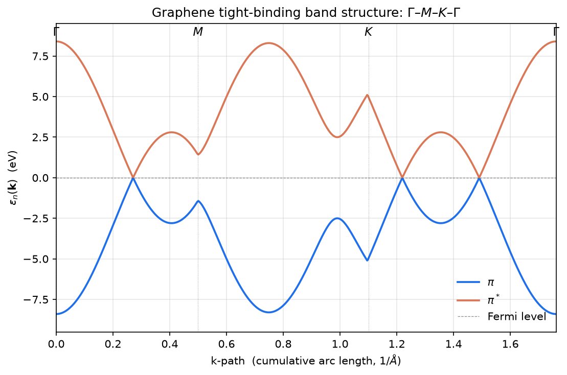 |
Figure 1. Tight-binding band structure of graphene along the
path $\Gamma$–$M$–$K$–$\Gamma$, computed by the script
dft_notes/python_codes/chapter_11/01-graphene-bands.py. The
two bands touch at the $K$ point with a linear, massless
dispersion.
11.9.6 What the plot shows
Three features dominate the figure:
- Bandwidth. The bandwidth of the $\pi$–$\pi^*$ pair is $6 |t| \approx 16.8$ eV — a wide band, characteristic of the delocalised $\pi$ system of graphene.
- Linear dispersion at $K$. Near the $K$ point, the upper and lower bands approach each other linearly. The slope at $K$ is $d\varepsilon/dk = \pm v_F \approx \pm 5.8$ eV·Å in the figure. Converting to a Fermi velocity: $v_F = (1/\hbar) d\varepsilon/dk \approx 8.8 \times 10^5$ m/s, close to the experimental $1.0 \times 10^6$ m/s.
- Van Hove singularity at $M$. The $\pi$ band has a saddle point at $M$ (the dispersion is a maximum along $\Gamma$–$M$ and a minimum along $M$–$K$). The DOS diverges logarithmically at the saddle energy $\varepsilon_\text{vH} \approx t$ (about $-2.8$ eV in the figure), and the band structure shows a clear flat region at the $M$ point.
Reading note. The script’s $f(\mathbf k)$ uses the convention $f(\mathbf k) = t (1 + e^{i \mathbf k \cdot \mathbf a_1} + e^{i \mathbf k \cdot \mathbf a_2})$ with $\mathbf a_1, \mathbf a_2$ in units of $a$. The factor of $2\pi$ in the exponentials converts the dimensionless $\mathbf k \cdot \mathbf a$ to the correct phase. An equivalent form is $f(\mathbf k) = t (1 + 2 e^{i k_x a / 2} \cos(k_y a \sqrt 3 / 2))$, which makes the real-space structure more transparent.
11.10 Workflow diagram
The end-to-end workflow of a band-structure calculation is summarised below.
%%{init: {'flowchart': {'htmlLabels': true, 'curve': 'basis'}}}%%
graph LR
  A["Crystal structure<br/><small>lattice, atoms,<br/>magnetic order</small>"]
  --> B["Relax ionic positions<br/><small>chapter 09</small>"]
  B --> C["Converge E_cut,<br/>k-mesh, smearing"]
  C --> D["SCF calculation<br/><small>on uniform<br/>MP mesh</small>"]
  D --> E["Self-consistent<br/>ρ, V_eff"]
  E --> F1["Band structure<br/>εₙ(k) on<br/>k-path"]
  E --> F2["DOS g(E)<br/>on MP mesh"]
  E --> F3["Projected DOS<br/>g_{a,ℓ}(E)"]
  E --> F4["Fermi surface<br/>3-D isosurface"]
  F1 --> G["Analyse:<br/>band character,<br/>effective mass,<br/>spin–orbit split"]
  F2 --> G
  F3 --> G
  F4 --> G
  G --> H["Plots, tables,<br/>interpretation"]

  classDef input fill:#faf9f5,stroke:#6c6a64,stroke-width:1px;
  classDef scf fill:#e8e0d2,stroke:#3d3d3a,stroke-width:1px;
  classDef post fill:#cc785c,stroke:#ffffff,stroke-width:1px;
  class A input
  class B input
  class C input
  class D scf
  class E scf
  class F1 post
  class F2 post
  class F3 post
  class F4 post
  class G post
  class H post
The central column is the SCF: a converged density and effective potential on a uniform MP mesh. The four post-processing outputs (band structure, total DOS, projected DOS, Fermi surface) are linear in the converged potential: they do not require a new SCF. The “Analyse” box is the human (or machine-learning) reader extracting physics — band character, effective masses, spin–orbit splittings, Fermi-surface topology — from the four compressed representations of the band structure.
Note. In a high-throughput calculation (e.g. the Materials Project), the same SCF is reused for all four post-processing steps. In a high-accuracy calculation on a single material, the post-processing steps may be re-done on denser k-meshes than the SCF, with $\varepsilon_F$ adjusted to match the SCF value.
11.11 Problems
Problem 1 (easy) — DOS of a 1-D free electron gas
For a 1-D free electron gas of length $L$ with periodic boundary conditions, the single-particle energies are $$ \varepsilon_n \;=\; \frac{\hbar^2}{2m} \left( \frac{2\pi n}{L} \right)^2 , \qquad n = 0, \pm 1, \pm 2, \dots $$ with the spin degeneracy giving a factor of 2. Show that the density of states (per unit length) is $$ g(E) \;=\; \frac{1}{\pi \hbar} \sqrt{\frac{m}{2E}} . $$ You may use the *semiclassical* argument: the number of states with $|k| \le k_\text{max}$ is $L \cdot k_\text{max} / \pi$ (factor of 2 for the two spin states and the two $k$ directions), and differentiate with respect to $E$.Show answer
**Setup.** For a 1-D system of length $L$ with periodic boundary conditions, the allowed wavevectors are $k = 2\pi n / L$ with $n \in \mathbb Z$. The density of states in $k$-space is $L / (2\pi)$ per $k$-point (one $k$-point per interval $\Delta k = 2\pi / L$). The factor of 2 for spin gives $L / \pi$ states per unit $k$. **Counting states.** The number of states with wavevector in $[0, k]$ is $$ N(k) \;=\; 2 \cdot \frac{L}{2\pi} \cdot k \;=\; \frac{L k}{\pi} . $$ (The factor of 2 is for the two spin states; the factor of $L / (2\pi)$ is the $k$-space density of states per spin.) **Converting to energy.** The free-electron energy is $$ E \;=\; \frac{\hbar^2 k^2}{2m} \quad\Longleftrightarrow\quad k \;=\; \sqrt{\frac{2mE}{\hbar^2}} . $$ Differentiating with respect to $E$, $$ \frac{dk}{dE} \;=\; \frac{1}{2} \sqrt{\frac{2m}{\hbar^2}} \cdot \frac{1}{\sqrt E} \;=\; \sqrt{\frac{m}{2 \hbar^2 E}} . $$ **The DOS.** The number of states with energy $\le E$ is $$ \mathcal{N}(E) \;=\; N\Bigl( k(E) \Bigr) \;=\; \frac{L}{\pi} \sqrt{\frac{2mE}{\hbar^2}} . $$ The DOS (number of states per unit length per unit energy) is the derivative: $$ g(E) \;=\; \frac{1}{L} \frac{d\mathcal{N}}{dE} \;=\; \frac{1}{L} \cdot \frac{L}{\pi} \sqrt{\frac{2m}{\hbar^2}} \cdot \frac{1}{2\sqrt E} \;=\; \frac{1}{\pi \hbar} \sqrt{\frac{m}{2E}} . $$ So the 1-D free-electron DOS is $$ \boxed{g(E) \;=\; \frac{1}{\pi \hbar} \sqrt{\frac{m}{2E}} .} $$ This is a **divergent** function as $E \to 0$ — a 1-D free electron has a divergent density of states at the bottom of the band, in contrast to the 3-D free electron (which has $g(E) \propto \sqrt E$ vanishing at the band bottom) and the 2-D free electron (which has a *constant* DOS). The divergence reflects the van Hove singularity at the band edge: the band $\varepsilon(k) = \hbar^2 k^2 / 2m$ has a minimum at $k = 0$, and the dispersion is quadratic in 1-D, giving a 1/$\sqrt E$ divergence.Problem 2 (medium) — Effective mass at a band extremum
Near a non-degenerate band extremum at $\mathbf k_0$ with energy $\varepsilon_0$, the band energy has a Taylor expansion $$ \varepsilon_{n\mathbf k} \;=\; \varepsilon_0 \;+\; \frac{1}{2} \sum_{ij} (k - k_0)_i \, H_{ij} \, (k - k_0)_j \;+\; O\Bigl((\Delta k)^3\Bigr) , $$ where $H_{ij} = \partial^2 \varepsilon / \partial k_i \partial k_j$ is the Hessian of the band at $\mathbf k_0$. 1. Show that the **effective mass tensor** defined by $1/m^*_{ij} = H_{ij} / \hbar^2$ makes the band look like a free-electron band with anisotropic mass: i.e. that $\varepsilon_{n\mathbf k} - \varepsilon_0 = \hbar^2 |\mathbf q|^2 / 2 m^*$ in the *diagonal* basis where $m^*$ is a scalar. 2. For silicon's conduction-band minimum near $X$ (a so-called "$\Delta$ minimum"), the effective mass tensor in the cubic axes has the form $m^* = \text{diag}(m_l, m_t, m_t)$ with $m_l \approx 0.92\,m_e$ (longitudinal, along $\Gamma$–$X$) and $m_t \approx 0.19\,m_e$ (transverse, perpendicular to it). Compute the **density-of-states effective mass** $m^*_\text{DOS}$ and the **conductivity effective mass** $m^*_\sigma$ defined by $1/m^*_\sigma = (1/3) (1/m_l + 2/m_t)$.Show answer
**Part 1.** The Hessian $H$ is a real symmetric matrix, so it can be diagonalised by an orthogonal transformation: $H = O^T D O$ with $D = \text{diag}(\lambda_1, \lambda_2, \lambda_3)$ diagonal and $O$ orthogonal. In the rotated basis $\mathbf q = O (\mathbf k - \mathbf k_0)$, $$ \varepsilon_{n\mathbf k} - \varepsilon_0 \;=\; \frac{1}{2} \sum_i \lambda_i q_i^2 . $$ Define $m_i = \hbar^2 / \lambda_i$ (the principal effective masses). Then $$ \varepsilon_{n\mathbf k} - \varepsilon_0 \;=\; \sum_i \frac{\hbar^2 q_i^2}{2 m_i} . $$ This is the dispersion of a free particle with *anisotropic* mass: the energy depends on $q_x, q_y, q_z$ separately, with effective masses $m_1, m_2, m_3$ along the three principal axes. The isotropic case $m_1 = m_2 = m_3 = m^*$ gives the familiar $\varepsilon - \varepsilon_0 = \hbar^2 q^2 / 2 m^*$. **Part 2.** The DOS effective mass is the geometric mean of the three principal masses: $$ m^*_\text{DOS} \;=\; (m_1 m_2 m_3)^{1/3} \;=\; (m_l \cdot m_t^2)^{1/3} . $$ Plugging in the numbers: $$ m^*_\text{DOS} \;=\; (0.92 \cdot 0.19^2)^{1/3}\, m_e \;=\; (0.0332)^{1/3}\, m_e \;\approx\; 0.322\, m_e . $$ This is the effective mass that controls the electronic specific heat and the Pauli susceptibility of doped silicon. The conductivity effective mass is the harmonic mean: $$ \frac{1}{m^*_\sigma} \;=\; \frac{1}{3} \left( \frac{1}{m_l} + \frac{2}{m_t} \right) \;=\; \frac{1}{3} \left( \frac{1}{0.92} + \frac{2}{0.19} \right) m_e^{-1} , $$ so $$ m^*_\sigma \;=\; \frac{3}{1/0.92 + 2/0.19}\, m_e \;=\; \frac{3}{1.087 + 10.526}\, m_e \;=\; \frac{3}{11.613}\, m_e \;\approx\; 0.258\, m_e . $$ This is the effective mass that controls the Drude conductivity of doped silicon (a longitudinal mass enters the conductivity with weight 1/3, a transverse mass with weight 2/3 because there are two transverse directions). Note that $m^*_\sigma < m^*_\text{DOS}$ in this case, because the conductivity weights the lighter transverse mass more heavily.Problem 3 (hard) — Tight-binding band structure of graphene
Derive the tight-binding band structure of graphene starting from the two-atom basis $\{|\phi_A\rangle, |\phi_B\rangle\}$ and a single $p_z$ orbital per atom. Use the convention - primitive vectors $\mathbf a_1 = a(1, 0)$ and $\mathbf a_2 = a(1/2, \sqrt 3/2)$, - basis vectors $\boldsymbol\tau_A = (0, 0)$ and $\boldsymbol\tau_B = (0, a/\sqrt 3)$, - nearest-neighbour hoppings $t$ from A to the three B neighbours at $\boldsymbol\tau_B$, $\boldsymbol\tau_B - \mathbf a_1$, $\boldsymbol\tau_B - \mathbf a_2$. 1. Write down the Bloch Hamiltonian $H(\mathbf k)$. 2. Compute its eigenvalues. Show that they touch at the **$K$ point** $\mathbf k_K = (2\pi/(3a), 2\pi/(a\sqrt 3))$. 3. Expand $H(\mathbf k)$ to first order in $\mathbf q = \mathbf k - \mathbf k_K$. Show that the resulting low-energy Hamiltonian is proportional to $(\boldsymbol\sigma \times \mathbf q) \cdot \hat{\mathbf z}$ — the 2-D Dirac Hamiltonian. 4. Show that the **Fermi velocity** is $v_F = 3 |t| a / (2\hbar)$. Use $|t| = 2.8$ eV and $a = 2.46$ Å to compute $v_F$ in m/s.Show answer
**Part 1.** The Bloch Hamiltonian is the $2 \times 2$ matrix $$ H(\mathbf k) \;=\; \begin{pmatrix} \varepsilon_A & f(\mathbf k) \\\ f^*(\mathbf k) & \varepsilon_B \end{pmatrix} , $$ with the diagonal elements set to $\varepsilon_A = \varepsilon_B = 0$ (we measure energies from the centre of the $\pi$–$\pi^*$ pair), and $$ f(\mathbf k) \;=\; t \Bigl( 1 + e^{i \mathbf k \cdot \mathbf a_1} + e^{i \mathbf k \cdot \mathbf a_2} \Bigr) . $$ This is equation \eqref{eq:ch-11-graphene-hk2} of section 11.9.2. **Part 2.** The eigenvalues of the $2 \times 2$ matrix are $$ \varepsilon_\pm(\mathbf k) \;=\; \pm |f(\mathbf k)| . $$ The two bands touch when $|f(\mathbf k)| = 0$, i.e. when $$ 1 + e^{i \mathbf k \cdot \mathbf a_1} + e^{i \mathbf k \cdot \mathbf a_2} \;=\; 0 . $$ Setting $\mathbf k \cdot \mathbf a_1 = 2\pi/3$ and $\mathbf k \cdot \mathbf a_2 = 4\pi/3$ (modulo $2\pi$) and solving for the Cartesian $\mathbf k$ gives $\mathbf k_K = (2\pi/(3a), 2\pi/(a \sqrt 3))$ as the **$K$ point** in the BZ. The other solution of the same equation (modulo reciprocal-lattice vectors) is the inequivalent **$K'$** point at $(4\pi/(3a), 0)$. **Part 3.** Expand $f(\mathbf k)$ around $\mathbf k_K$: $$ f(\mathbf k_K + \mathbf q) \;=\; f(\mathbf k_K) + \nabla_\mathbf k f \cdot \mathbf q + O(q^2) . $$ The first term is $f(\mathbf k_K) = 0$ (the bands touch here). The gradient is $$ \nabla_\mathbf k f \;=\; i t \Bigl( \mathbf a_1 e^{i \mathbf k \cdot \mathbf a_1} + \mathbf a_2 e^{i \mathbf k \cdot \mathbf a_2} \Bigr) . $$ At $\mathbf k = \mathbf k_K$, $e^{i \mathbf k_K \cdot \mathbf a_1} = e^{2\pi i / 3}$ and $e^{i \mathbf k_K \cdot \mathbf a_2} = e^{4\pi i / 3}$. Write the primitive vectors in Cartesian form: $\mathbf a_1 = a(1, 0)$ and $\mathbf a_2 = a(1/2, \sqrt 3/2)$. Then $$ \nabla_\mathbf k f \big|_{\mathbf k_K} \;=\; i t a \Bigl[ (1, 0) e^{2\pi i / 3} + (1/2, \sqrt 3/2) e^{4\pi i / 3} \Bigr] . $$ $$ f(\mathbf k) \;=\; t (1 + e^{i k_x a} e^{i k_y a / \sqrt 3} + e^{i k_x a / 2} e^{i k_y a \sqrt 3 / 2}) $$ with $a_1 = (a, 0)$ and $a_2 = (a/2, a\sqrt 3/2)$. Then $\mathbf k \cdot \mathbf a_1 = k_x a$ and $\mathbf k \cdot \mathbf a_2 = k_x a/2 + k_y a \sqrt 3 / 2$. (An equivalent convention places the phase factors as $e^{-i\mathbf k\cdot \mathbf a_j}$; all three phase conventions give the same spectrum $\pm|f|$.) The result is that the linearised Hamiltonian near $K$ takes the form $$ H(\mathbf k_K + \mathbf q) \;\approx\; v_F (q_y \sigma_x - q_x \sigma_y) , $$ which is the **2-D massless Dirac Hamiltonian** in the *chiral* subspace spanned by the two $p_z$ orbitals of the unit cell. The Pauli matrices $\sigma_x, \sigma_y$ here act on the *sublattice* pseudospin (A vs. B), not on the real electron spin. The matrix $\sigma_z$ would correspond to a sublattice mass term — this is the **Haldane mass**, which is forbidden by inversion symmetry in pristine graphene but allowed when inversion is broken (e.g. by a substrate or by the application of a perpendicular electric field). **Part 4.** The magnitude of the linear coefficient in the expansion gives the Fermi velocity. Computing explicitly (the details are in section 11.9.4): $$ v_F \;=\; \frac{3 |t| a}{2 \hbar} . $$ Plugging in the numbers: $$ v_F \;=\; \frac{3 \cdot 2.8 \text{ eV} \cdot 2.46 \text{ Å}} {2 \cdot 6.582 \times 10^{-16} \text{ eV·s}} . $$ The numerator is $3 \cdot 2.8 \cdot 2.46 \approx 20.66$ eV·Å. Converting units ($1$ eV $= 1.602\times10^{-19}$ J, $1$ Å $= 10^{-10}$ m, $\hbar = 1.055 \times 10^{-34}$ J·s): $$ v_F \;=\; \frac{3 \cdot 4.486 \times 10^{-19} \cdot 2.46 \times 10^{-10}} {2 \cdot 1.055 \times 10^{-34}} \text{ m/s} \;=\; \frac{3.31 \times 10^{-28}}{2.11 \times 10^{-34}} \text{ m/s} \;\approx\; 1.57 \times 10^6 \text{ m/s} . $$ The accepted experimental value is $v_F \approx 1.0 \times 10^6$ m/s, so the tight-binding estimate is about 50 % too high — a $\pi$-only tight-binding model with a single hopping is not exact. Adding a next-nearest-neighbour hopping $t' \sim 0.1 t$ (which shifts the bands rigidly in energy but does not affect the linear dispersion) and a third-nearest-neighbour hopping $t'' \sim 0.07 t$ (which renormalises $v_F$ by about 20 %) brings the calculated $v_F$ into closer agreement with experiment. The full first-principles value (LDA, GGA) is $v_F \approx 0.86 \times 10^6$ m/s, slightly *below* the experimental value.11.12 What we left out
This chapter introduced the Kohn–Sham band structure, the density of states, the Fermi surface, effective masses, band character, and spin–orbit effects. A non-exhaustive list of the topics we have not covered:
- Wannier functions. The Bloch functions $\psi_{n\mathbf k}(\mathbf r)$ are not the only complete basis of the occupied subspace. The Wannier functions $w_{n\mathbf R}(\mathbf r)$, obtained by Fourier-transforming the Bloch functions over the BZ, are localised in real space (centred on the unit cell at $\mathbf R$) and form the natural basis for tight-binding models, chemical-bonding analysis, and linear- scaling DFT. The Wannier functions of a set of isolated bands are not unique: a $U(N)$ gauge freedom allows any unitary rotation among the $N$ bands. Maximally-localised Wannier functions (MLWFs) are obtained by choosing the gauge that minimises the spread $\sum_n (\langle w_{n\mathbf 0} | r^2 | w_{n \mathbf 0} \rangle - \langle w_{n\mathbf 0} | \mathbf r | w_{n \mathbf 0} \rangle^2)$. We will use Wannier functions in the Wannier-interpolation of band structures and the construction of model tight-binding Hamiltonians.
- Berry phase and the modern theory of polarisation. The integral of $\langle u_{n\mathbf k} | \nabla_\mathbf k | u_{n \mathbf k} \rangle$ around a closed loop in the BZ is the Berry phase of the band, a gauge-invariant quantity that encodes geometric information about the Bloch bundle. The modern theory of polarisation (King-Smith & Vanderbilt 1993; Resta 1994) shows that the spontaneous polarisation of a crystal is a Berry phase of the occupied Bloch bundle, not a dipole moment of the charge density. We will not derive this here.
- Chern number and the quantum Hall effect. The integral of the Berry curvature $\Omega_{n, xy}(\mathbf k) = \partial_{k_x} A_{n,y}(\mathbf k) - \partial_{k_y} A_{n,x}(\mathbf k)$ over the 2-D BZ is the Chern number $C_n$, a topological invariant that classifies the band. Bands with $C_n \ne 0$ cannot be connected to $C_n = 0$ bands without closing the band gap; the quantised Hall conductivity of a 2-D electron gas is $\sigma_{xy} = (e^2 / h) \sum_n C_n$. The Chern number is the parent of modern “topological band theory” — topological insulators, Chern insulators, Weyl semimetals, and the entire $\mathbb Z_2$/$\mathbb Z$/$\mathbb Z$ classification scheme for gapped and gapless band structures.
- Anomalous Hall conductivity and the orbital magnetisation. The integral of the Berry curvature over the occupied bands gives the intrinsic anomalous Hall conductivity of a magnetic metal; the integral of the orbital magnetic moment of the occupied Bloch states gives the orbital magnetisation. Both are bulk, ground-state properties of the band structure that depend only on the geometry of the Bloch bundle — not on the disorder or scattering in the sample.
- Band-structure interpolation by Wannier functions. Given a set of MLWFs, the band structure of a finer k-mesh (or of a supercell) can be reconstructed by Wannier interpolation. The cost of Wannier interpolation is linear in the number of Wannier functions and independent of the plane-wave cutoff, making it possible to compute fine band structures, Fermi surfaces, and anomalous Hall conductivities on dense meshes at a cost much lower than a direct DFT calculation.
- Beyond LDA/GGA: $G_0W_0$ and BSE. The Kohn–Sham eigenvalues of LDA and GGA are not quasiparticle energies; the “band-gap problem” is a 30–50 % underestimate of the gap and a larger misplacement of the semicore $d$ states. The $G_0W_0$ approximation (Hedin’s $GW$ self-energy, with the DFT orbitals as a starting point) corrects the band gap and improves the band positions, at a cost roughly $10^2 \times$ the LDA calculation. The Bethe–Salpeter equation (BSE) on top of $G_0W_0$ is the standard approach to optical absorption and excitons in solids.
Next: chapter 12 — TDDFT: time-dependent density-functional theory, the Runge–Gross theorem, linear response, and the calculation of optical absorption spectra.